Help ?

IGMIN: We're glad you're here. Please click 'create a new query' if you are a new visitor to our website and need further information from us.

If you are already a member of our network and need to keep track of any developments regarding a question you have already submitted, click 'take me to my Query.'

Search

Organised by  IgMin Fevicon

Regional sites

Browse by Subjects

Welcome to IgMin Research – an Open Access journal uniting Biology, Medicine, and Engineering. We’re dedicated to advancing global knowledge and fostering collaboration across scientific fields.

Members

We are dedicated to creating intersections where disciplines meet to expand knowledge.

Articles

We are dedicated to creating intersections where disciplines meet to expand knowledge.

Explore Content

We are dedicated to creating intersections where disciplines meet to expand knowledge.

Identify Us

We are dedicated to creating intersections where disciplines meet to expand knowledge.

IgMin Corporation

Welcome to IgMin, a leading platform dedicated to enhancing knowledge dissemination and professional growth across multiple fields of science, technology, and the humanities. We believe in the power of open access, collaboration, and innovation. Our goal is to provide individuals and organizations with the tools they need to succeed in the global knowledge economy.

Publications Support
[email protected]
E-Books Support
[email protected]
Webinars & Conferences Support
[email protected]
Content Writing Support
[email protected]
IT Support
[email protected]

Search

Select Language

Explore Section

Content for the explore section slider goes here.

194 of 194
Assessment of Thermal Uniformity of Heating Plates Using a Thermal Imaging Camera
Leszek Jurdziak, Aleksandra Rzeszowska and Ryszard Błażej
END
Abstract

Abstract at IgMin Research

We are dedicated to creating intersections where disciplines meet to expand knowledge.

Engineering Group Research Article Article ID: igmin305

A Unified Mobility Model for Semiconductor Devices and Sensors, Including Surface Hydrodynamic Viscosity

Biomedical Engineering DOI10.61927/igmin305 Affiliation

Affiliation

    Ain-Shams University Engineering College, 15117 Abbasya, Cairo, Egypt

14
VIEWS
12
DOWNLOADS
Connect with Us

Abstract

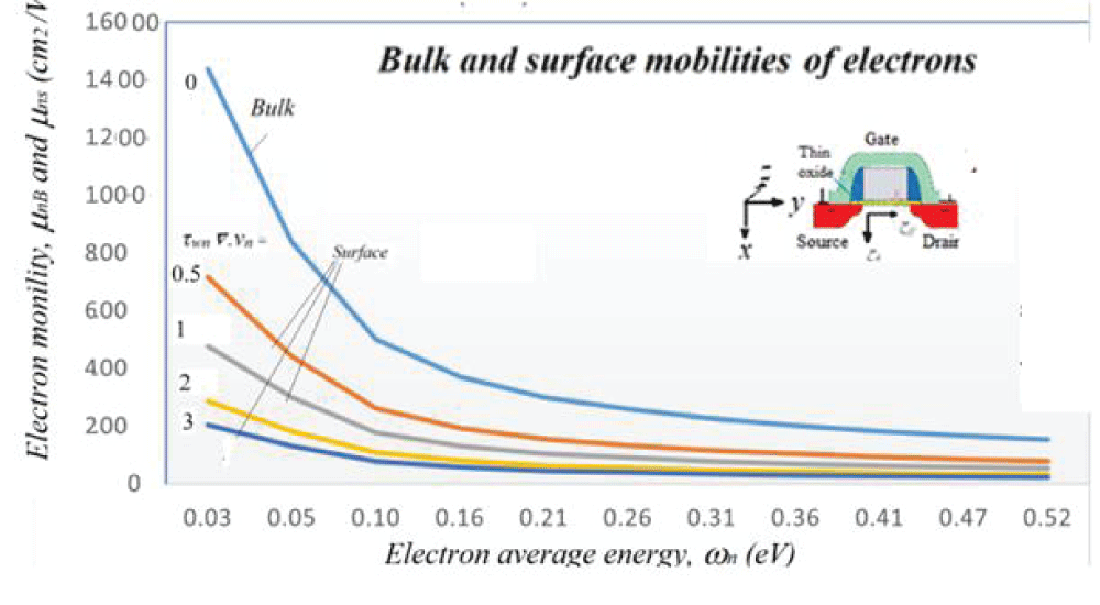
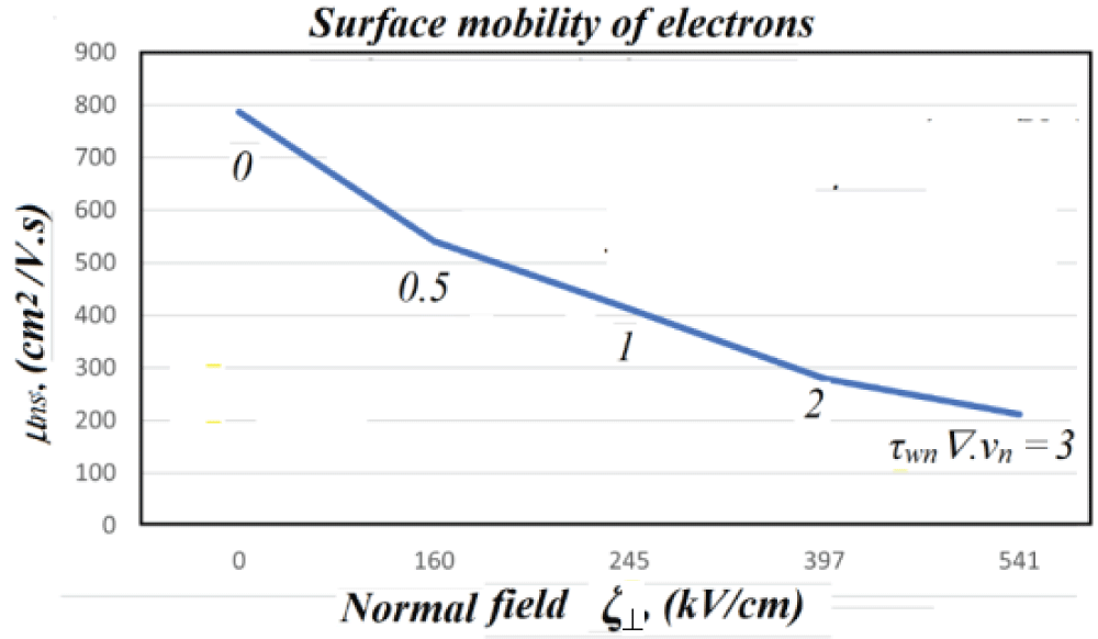
In this paper we present a physics-based model for hot carrier surface mobility in semiconductor devices and sensors which incorporates the band structure and interface/surface effects. This model can be utilized within the generalized hydrodynamic model (HDM), for semiconductor device and sensor simulation [1]. The proposed non-local surface mobility model is essentially needed in the hydrodynamic transport modelling of hot carriers as an energy-dependent model. Unfortunately, most of the involved parameters in the hydrodynamic simulation of semiconductor devices and sensors are obtained from Monte Carlo simulation in the bulk of a homogenous semiconductor. However, the correct simulation of the dynamic behaviors of hot carrier transport across semiconductor surfaces and junctions, needs to consider the main variable gradients, such as the carrier density, energy (or temperature) and velocity gradients. In particular, the velocity gradient plays a significant role in the transport of hot carriers in 2D electron/hole gas devices. Therefore, our mobility model focuses on the role of velocity gradients of hot carriers and the underlying carrier gas viscosity, to interpret the well-known surface mobility reduction, near the Si/SiO2 interface in nano devices and nano sensors. Unlike previous surface mobility models, which are primarily based on the local electric field and fitting of experimental data, our model is physics-based on the hot carrier energy and velocity gradients. Therefore, our model is also considered truly non-local and fully hydrodynamic.

Figures

References

    1. El-Saba MH. Transport of Information-Carriers in Semiconductors and Nanodevices. PA, USA: IGI Global Publisher; 2017. Available from: https://www.igi-global.com/book/transport-information-carriers-semiconductors-nanodevices/173677
    2. Hess K, Leburton JP, Ravaioli U, editors. Hot Carriers in Semiconductors. Springer; 1996.
    3. Fischetti MV, Vandenberghe WG. Overview of Quantum-Transport Formalisms. In: Advanced Physics of Electron Transport in Semiconductors and Nanostructures. Graduate Texts in Physics. 361-380; 2016.
    4. Martinez, Bescond M, Barker JR, Svizhenko A, Anantram MP, Millar C, Asenov A. A self-consistent full 3-D real-space NEGF simulator for studying nonperturbative effects in nano-MOSFETs. IEEE Trans Electron Devices. 2007;54(9):2213–2222.
    5. Cerciganani A. The Boltzmann Equation and its Applications. Vienna: Springer-Verlag; 1988.
    6. Rupp K. Deterministic Numerical Solution of the Boltzmann Transport Equation [Ph.D. Dissertation]. TUV, Wien; 2011. Available from: http://www.iue.tuwien.ac.at/phd/rupp/
    7. Jacoboni C, Lugli P. The Monte Carlo Method for Semi-conductor Device Simulation. Springer Science and Business Media; 2012.
    8. Vasileska D, Raleva K, Goodnick SM, Ringhofer C, Ahmed SS, Ashraf N, Hossain A, Hathwar R, Ashok A, Padmanabhan B. Monte Carlo Device Simulations. In: Applications of Monte Carlo Method in Science and Engineering. InTech; 2011. DOI: 10.5772/16190
    9. Vasicek M. Advanced Macroscopic Transport Models [Dissertation]. Technische Universität Wien; 2009.
    10. El-Saba MH, Taha MS. An Ultimate Hydrodynamic Model for Semiconductor Devices, Including Band Structure and Surface Effects. Sensors and Actuators Magazine. 2024;267(4).
    11. Sabbah AJ, Riffe DM. Femtosecond Pump-Probe Reflectivity Study of Silicon Carrier Dynamics. Phys Rev B. 2002;66:165217-165228.
    12. Takagi S, Toriumi A, Iwase M, Tango H. On the Universality of Inversion Layer Mobility in Si MOSFET’s: Part I – Effects of Substrate Impurity Concentration. IEEE Transactions on Electron Devices. 1994;41(12):2357-2362.
    13. EL-SABA MH. Hydrodynamic Modeling and Simulation of Hot Carrier Transport Phenomena and Impact Ionization in Semiconductor Devices [Ph.D. Dissertation]. INSA Lyon, France; 1993. Order No.93 ISAL 0072.
    14. Takagi S, Toriumi A, Iwase M, Tango H. On the universality of inversion layer mobility in Si MOSFET’s: part II—effects of surface orientation. IEEE Trans Electron Dev. 1994;41(12):2363–2368.
    15. Gardner C. The quantum hydrodynamic model for semiconductor devices. SIAM Journal on Applied Mathematics. 1994;54(2):409–427.
    16. Spinelli AS. Self-consistent 2-D model for quantum effects in n-MOS transistors. IEEE Trans Electron Devices. 1998.
    17. Ferry DK, Ramey S, Shifren L, Alkis E. The Effective Potential in Device Modeling: The Good, the Bad and the Ugly. Journal of Comp Electron. 2002;1(1):9–65.
    18. Asenov A, Brown AR, Watling JR. Quantum Corrections in the Simulation of Decanano MOSFETs. Solid-State Electron. 2003;47(7):1141-1145.
    19. Yue C, Agostinelli V, Yeric GM, Tasch A. Improved universal MOSFET electron mobility degradation models for circuit simulation. IEEE Transactions on Computer Aided Design. 1993;12(10).
    20. Yamaguchi K. Field-Dependent Mobility Model for Two-Dimensional Numerical Analysis of MOSFET's. IEEE Trans Electron Devices. 1979;26:1068-1074.
    21. Caughey DM, Thomas RE. Carrier Mobilities in Silicon Empirically Related to Doping and Field. Proc IEEE. 1967:2192–93.
    22. Nishida T, Sah CT. A physically based mobility model for MOSFET numerical simulation. IEEE Transactions on Electron Devices. 1987;34(2).
    23. Donetti L, Gamiz F, Rodriguez N, Godoy A. Hole mobility in ultrathin double-gate SOI devices: the effect of acoustic phonon confinement. IEEE electron device letters. 2009;30(12):1338-1340.
    24. Darwish MN, Lentz JL, Pinto MR, Zeitzoff PM, Krutsick TJ, Vuong HH. An Improved Electron and Hole Mobility Model for General Purpose Device Simulation. IEEE Trans Electron Dev. 1997;44(9):1529-1538.
    25. Klassen DB. A unified mobility model for device simulation-Part I: Model equations and concentration dependence. Solid-State Electron. 1992;35(7):953-959.
    26. Lombardi C, Manzini S, Saporito A, Vanzi M. A physically based mobility model for numerical simulation of nonplanar devices. IEEE Trans Computer-Aided Design. 1988;7:1164–1171.
    27. Gamiz F, Lopez-Villanueva JA, Banqueri J, Carceller J, Cartujo P. Universality of electron mobility curves in MOSFET’s: A Monte Carlo study. IEEE Trans Electron Devices. 1995;42:258.
    28. Esseni D. On the Modeling of Surface Roughness Limited Mobility in SOI MOSFETs and its Correlation to the Transistor Effective Field. IEEE Trans Electron Devices. 2004;51:394-401.
    29. Weber O, Takagi S. New Findings on Coulomb Scattering Mobility in Strained-Si nFETs and its Physical Understanding. Symposium on VLSI Technology Digest. 2007:130-131.
    30. Gamiz F, López-Villanueva JA, Roldan JB. Monte Carlo simulation of electron transport properties in extremely thin SOI MOSFET's. IEEE Transactions on Electron Devices. 2009;45(5):1122–1126.
    31. Naydenov K, Donato N, Udrea F. An advanced physical model for the Coulombic scattering mobility in 4H-SiC inversion layers. Journal of Applied Physics. 2020;127:194504.
    32. Balaguer M, Roldan JB, Donetti L, Gamiz F. Inversion charge modeling in n-type and p-type Double-Gate MOSFETs including quantum effects: The role of crystallographic orientation. Solid-state electronics. 2012;67(1):30-37.
    33. Reggiani S, Valdinoci M, Colalongo L, Baccarani G. A Unified Analytical Model for Bulk and Surface Mobility in Si n-and p-Channel MOSFET's. Proc European Solid-State Device Research Conf. 1999;1.
    34. El-Saba MH. Accurate Estimation of Electron Velocity Overshoots in Sub-0.1 micron Silicon Structures and MOSFET Devices. Proceedings of the 15th Radio Science Conference, NRSC '98. 1998:D2/1 - D2/5.
    35. El-Saba MH. Investigation of Hot Carrier Repelling Effect in Semiconductor Devices, Using an Analytical Solution of the Hydrodynamic Model. IEEE Trans Electron Devices. 2006;53(7):1615-1622.
    36. El-Saba MH. Yet another Hydrodynamic Model for Silicon Devices with Correlated Parameters. Scientific & Academic Publishers, Microelectronic Devices and Solid-State Electronics. 2012;1(5):118-147.
    37. Hansch W, Miura-Mattausch M. The Hot-Electron Problem in Small Semiconductor Devices. Journal of Applied Physics. 1986;60(2):650-656.
    38. Gonzalez B, Palankovski V, Kosina H, Hernandez A, Selberherr S. An energy relaxation time model for device simulation. Solid-state electronics. 1999;43(9):1791-1795.
    39. Alekseev PS, Dmitriev AP. Viscosity of two-dimensional electrons. arXiv:2007-02291v4 [cond-mat-ms, es-hall]. 2021.
    40. Vasileska D, Goodnick S, Klimeck G. Computational Electronics: Semi-Classical and Quantum Device Modeling and Simulation. CRC Press; 2010.
    41. El-Saba MH, Taha MS. Hydrodynamic Modeling of the 2DEG/2DHG viscosity, as a function of the electron/hole temperature. To be published. 2023.
    42. Watt JT, Plummer JD. Universal Mobility-Field Curves for Electrons and Holes in MOS Inversion Layers. 1987 Symposium on VLSI Technology. Digest of Technical Papers, Karuizawa, Japan. 1987:81-82.
    43. Sasso G, Rinaldi N, Matz G, Jungemann C. Accurate Mobility and Energy Relaxation Time Models for SiGe HBTs Numerical Simulation. 2009 International Conference on Simulation of Semiconductor Processes and Devices, San Diego, CA, USA. 2009:1-4.
    44. Dolgopolov VT, Shashkin AA, Dorozhkin SI, Vyrodov EA. Energy relaxation time in a two-dimensional electron gas at a (001) surface of silicon. JETP, Theor. Fi. 1985;89:2113-2123.
    45. Sho S, Odanaka S. A quantum energy transport model for semiconductor device simulation. Journal of Computational Physics. 2013;235:486–496.
    46. Wang X, Xu X, Wang H. Analytical model for uniaxial strained Si inversion layer electron effective mobility. IET Circuits, Devices & Systems. 2019;13(3):414-419.
    47. El-Saba MH. Problems Related to the Semiconductors Hydrodynamic Model: Modeling the Carrier-Heat Flux Term. Proc of the 8th Int Conf on Microelectronics-ICM, M. El-Masry (Ed.), Cairo. 1996:162–166.
    48. Mir SH, Yadav VK, Singh JK. Recent Advances in the Carrier Mobility of Two-Dimensional Materials: A Theoretical Perspective. ACS Omega. 2020;5(24):14203-14211.

Similar Articles

System for Detecting Moving Objects Using 3D Li-DAR Technology
Md. Milon Rana, Orora Tasnim Nisha, Md. Mahabub Hossain, Md Selim Hossain, Md Mehedi Hasan and Md Abdul Muttalib Moon
DOI10.61927/igmin167
Use of Augmented Reality as a Radiation-free Alternative in Pain Management Spinal Surgeries
Songyuan Lu, Jingwen Hui, Eric Lee, Darin Tsui, Farshad M Ahadian and Frank E Talke
DOI10.61927/igmin236
Investigation of Lateral Vibrations in Turbine-generator Unit 5 of the Inga 2 Hydroelectric Power Plant
André Mampuya Nzita, Edmond Phuku Phuati, Robert Muanda Ngimbi, Guyh Dituba Ngoma and Nathanaël Masiala Mavungu
DOI10.61927/igmin173

Why publish with us?

  • Global Visibility – Indexed in major databases

  • Fast Peer Review – Decision within 14–21 days

  • Open Access – Maximize readership and citation

  • Multidisciplinary Scope – Biology, Medicine and Engineering

  • Editorial Board Excellence – Global experts involved

  • University Library Indexing – Via OCLC

  • Permanent Archiving – CrossRef DOI

  • APC – Affordable APCs with discounts

  • Citation – High Citation Potential

Submit Your Article

Advertisement