IGMIN: We're glad you're here. Please click 'create a new query' if you are a new visitor to our website and need further information from us.
If you are already a member of our network and need to keep track of any developments regarding a question you have already submitted, click 'take me to my Query.'
Welcome to IgMin Research – an Open Access journal uniting Biology, Medicine, and Engineering. We’re dedicated to advancing global knowledge and fostering collaboration across scientific fields.
At IgMin Research, we bridge the frontiers of Biology, Medicine, and Engineering to foster interdisciplinary innovation. Our expanded scope now embraces a wide spectrum of scientific disciplines, empowering global researchers to explore, contribute, and collaborate through open access.
Welcome to IgMin, a leading platform dedicated to enhancing knowledge dissemination and professional growth across multiple fields of science, technology, and the humanities. We believe in the power of open access, collaboration, and innovation. Our goal is to provide individuals and organizations with the tools they need to succeed in the global knowledge economy.
IgMin Publications Inc., Suite 102, West Hartford, CT - 06110, USA
There is constructed a qualitative model of the electrical conductivity of semiconductors irradiated with sufficiently high-energy particles. At certain conditions (irradiation temperature and dose, and subsequent thermal treatment), high-energy particles fluence, in addition to primary and secondary point radiation defects, forms a number of nano-sized disordered regions, highly conductive (“metallic”) compared to the semiconductor matrix. Their high total volume fraction can lead to the charge major carriers’ effective Hall mobility significantly exceeding that of the matrix. Due to elastic stresses created by these disordered inclusions, a high concentration of point radiation defects tends to form defective shells. In certain temperature ranges, such nanosized core-shell structures act as capacitors storing the electric charge sufficient for the Coulomb blockade of the major current carriers. Transformation of high-conductive inclusions into low-conductive (“dielectric”) ones manifests in a noticeable decrease in effective Hall mobility. The proposed model qualitatively explains all the experimental data available on single-crystalline n- and p-type silicon irradiated with high-energy electrons and protons and isochronously annealed.
Irradiated semiconductors, mainly, silicon structures are widely used in micro- and nanoelectronics. In the literature, there is available a huge number of reports on their irradiation-induced morphology and related physical-electrical properties.
A review [1] of the research into processes and mechanisms of defect formation in materials irradiated by fast particles shows that the nature and morphology of their defective tracks depend on the material type and on the energy density transferred to its electron subsystem. The relaxation of high electronic excitations dominates the track formation process.
Characteristics of complex defects in semiconductors were calculated [2] by the method of minimizing the free energy for the crystal considering the influence electron subsystem on the impurity solubility. The modeling of solidus curves is carried out in terms of binary association and clustering. The numerical calculations of the point defects, vacancies, and divacancies accumulation kinetics for different radiation conditions are conducted [3] based on the so-called diffusion–coagulation model without weak-diffusion approximation needed at the model analytic realization. The theoretical developments [4] of computer simulation techniques for studying radiation effects in materials, mainly silicon, are closely intertwined with associated experiments. These methods either deal directly with the primary radiation damage generation or defects and phase changes that typically occur due to radiation. The methods proposed are RE (Rate Equations), MCN (Monte Carlo Neutronics), MMC (Metropolis Monte Carlo), KMC (Kinetic Monte Carlo), MD (Molecular Dynamics), BCA (Binary Collision Approximation), DDD (Discrete Dislocation Dynamics), TD–DFT (Time-Dependent Density Functional Theory), FEM (Finite Element Modelling), etc.
A Monte Carlo method used [5] to obtain the detailed structure of RDs (Radiation Defects) cluster formed after silicon irradiation by fast neutrons showed that the distribution of corresponding subclusters is not uniform. In this way represented data – cluster structure, their spatial distribution, and size-distribution function for subclusters – can be used for simulation of high-energy electron transport in submicron semiconductor devices under irradiation. Another Monte Carlo simulation [6,7] of the detailed structure of DRs (Disordered Regions) produced by fast neutron radiation in Si (as well as GaAs, SiGe, and GaN) showed that high electrical fields in the submicron solid state devices generate the hot electrons, which can penetrate between separated subclusters of a DR. In particular, in Si, it causes a strong field dependence of the conduction electrons scattering by DRs. Using the MD method the formation of a DR of defects in bulk silicon is simulated [8] for different energies of the primary recoil atom.
According to the model of irradiation-induced disordering of semiconductors [9], the DRs capable of self-annealing are stabilized by self-localized electronic excitations such as electrons, holes, and excitons. Their pulsed annealing occurs through the recombination of the electronic stoppers and thus dispersal of disordered regions takes place. This model agrees well with the experiments on amorphization and laser pulse annealing. In the model of DRs generation as a result of Frenkel interstitial atom–vacancy pairs separation [10,11], the probability of separation depends on pair neutral and charged states, temperature, and Fermi level position in the band gap and, therefore, the primary RDs concentration. This model allows us to define the radius and the mean number of vacancies of a disordering region. Calculation of the depth distribution profiles of primary RDs created by protons in silicon. DR’s parameters dependence on the proton energy shows that for the maximum created by protons, DRs distribution is always spatially separated from the maxima of distributions of interstitial Si, vacancies, and divacancies, which allows differential modification of superficial and volumetric properties of silicon structures by irradiation. The theory of void nucleation in irradiated materials [12] has been critically analyzed and further developed the standard theory, which can overestimate the rate of empty void nucleation in some irradiated materials. The revision-based adequate interpretation of irradiation tests showed that the number of void nuclei is determined by the concentration of vacancies in the irradiated material.
When analyzing experimental data on RDs in n-Si based on theoretical models, the point radiation defects concentration
(1)
assumed to be the difference between carrier concentrations in crystals at room temperature before n0 and after irradiation nD with fast electrons dose of D, is demonstrated [13] to follow the exponential law
(2)
irrespective of electron energy (D0 is a constant). The introduction rate ∆Ndef/∆D of radiation defects, according to their particular character, has to decrease exponentially with the dose delivered. And the rate of carrier mobility versus radiation dose also decreases exponentially. The higher electrical conductivity of semiconducting silicon single crystals both n- and p-types during their electron irradiation under common conditions with respect to after-irradiation value is explained [14] by ionization and capture mechanisms resulting in the formation of non-equilibrium carriers in the form of hole–electron pairs. Irradiation induces Si different RDs, concentration and character of which highly depend on sample temperature and radiation dose. At high temperatures, the generated RDs are stable and their concentration depending on sample temperature and dose reveals a non-monotonous character. The efficiency of RDs introduction into n-Si shows maxima with an increase of electron beam dose. According to the analysis, the formation of deep centers with energetic levels at EC–0.40 and 0.53 in n-Si, and 0.56 and 0.66 eV in p-Si, which are responsible for decreasing and degradation of the conductivity. By the use of PBW (Proton Beam Writing) technology single-crystalline n-Si was irradiated [15] with hydrogen ions H+ of energy 1.5 MeV and an integrated dose of 2·1015 р/cm2. In general, the temperature dependence of the sample resistance after irradiation is significantly different from the typical one.
According to the Hall measurements-based study [16] of interactions of shallow group-V donor or group-III acceptor impurities with primary defects in oxygen O and carbon C lean moderately doped silicon subjected to irradiation with 0.9 MeV electrons, Co gamma-rays, and 15 MeV protons, the losses of the shallow donor or acceptor states in the irradiated Si are indicative of their removal rates that can be used for estimation of production rates of primary defects interacting with these dopants. Investigation of annealing processes of vacancy–impurity atom pairs in moderately doped n-type silicon grown subjected to 0.9 MeV electron irradiation by means of Hall measurements showed [17] that the Fermi level position at annealing stages between 100 and 260 °C plays an important role in recovery of the electrical properties of irradiated samples. The first annealing stage between 100 and 160 °C is associated with limited migration of vacancy–impurity atom pairs and their trapping by free dopant phosphorus atoms. As a consequence, complexes of vacancy–two impurity atoms appear. They are stable up to 600 °C. The complete restoration of the electrical parameters of irradiated samples is observed at 700 °C.
There are considered effects of various factors such as background impurity oxygen [18], donor dopant phosphorus P [19,20], acceptor dopant boron B [21,22], annealing temperature [23,24], IR (InfraRed) illumination [25], irradiation dose [26], etc. on electron Hall mobility in proton irradiated silicon. The electric resistance and effective carrier mobility in polycrystalline silicon are calculated [27] as functions of temperature and photoexcitation level. These theoretical results are in agreement with existing experimental data.
Analysis [28] of the progress in the modification of semiconductors by proton beams in fields such as proton-enhanced diffusion, ion-beam mixing, and formation of porous layers showed that this method of doping has a higher potential in monitoring the properties of semiconductor materials and designing devices of micro- and nanoelectronics compared to the conventional doping techniques such as thermal diffusion, epitaxy, and ion implantation. By comparing the generation–recombination lifetime degradation of silicon junction diodes by 10 MeV proton irradiation with the introduction of the radiation-induced deep levels, the n-type Si was found [29] to be more prone to high-energy proton irradiation damage than p-type material. From the electrical diode characteristics, it is derived that the dominant generation center in both n- and p-type float-zone Si is level at EC –0.42 eV (approximately 0.12 eV from the midgap position).
By studying [30] the effect of the formed p+-layer thickness on the efficiency of the formation of radiation recombination centers in the p+–n–n+ transition of diffusion diodes under irradiation with 4–6 MeV electrons it is detected that the radiation centers with levels of EC–0.17, 0.23, and 0.39, 0.44 eV should be attributed, respectively, to A-center, two different charge states of the divacancy, and E-center.
Irradiation by low-energy protons leads to variations in electrical, optical, and other properties of a semiconductor structure surface layer. It gives additional possibilities to modify semiconductor devices [31]. Double-sided silicon photoelectric structures n+–p–p+ are irradiated by protons with an energy of 40 or 180 keV at a temperature of 83 K. To explain the observed regularities of varying current-voltage characteristic parameters and transmission coefficients, the distributions of average numbers of interstitial silicon atoms, vacancies, divacancies, and DRs formed under these conditions per length unit of the projected path by one proton in the n+–p junction space-charge region diffusion layer are calculated. The number of radiation-induced defects at the maximum of the spatial distribution in the n-type region is found to be much smaller than in the p-type region.
The purpose of this work is to construct a qualitative model of DRs, which allows us to estimate the electrical-physical parameters of semiconductor materials and structures irradiated with high doses of high-energy particles. The introduced theoretical model is based on a systematic experimental study of n- and p-Si samples irradiated with protons and electrons, respectively.
It has been studied the zone-melted silicon crystals (with an oxygen content of ∼1016 cm–3 and density of growth dislocations of 103–104 cm–2) with n- and p-type conductivities doped with phosphorus P and boron B, respectively, with approximately the same concentration of the major current carriers of 6·1013 cm–3. Test single crystals are cut out in the form of bars of dimensions 1×3×10 mm with the largest facet (111).
Samples of n- and p-types are irradiated at room temperature, respectively, with protons and electrons of energies 25 and 8 MeV and doses of 8.1·1012 and 1.0·1015 cm–2, respectively. They are isochronously annealed in the temperature range of 80–600 °C in steps of 10 °C with an exposure time of 10 min at a fixed temperature. The annealing temperature is determined by a chromel–alumel thermocouple. After each annealing cycle, Hall measurements of the current carriers’ concentration and mobility were carried out in the range from the nitrogen boiling point to room temperature. The change in a sample temperature was controlled by a copper–constantan thermocouple. The Ohmic contacts, necessary for measuring the electrical parameters of silicon samples, are created by rubbing aluminum into their surfaces.
The energy levels of the RDs were determined from the temperature-dependences of the Hall concentration nH and mobility µH of current carriers measured in this way. Features of the analysis depend on the degree of compensation of a tested sample. For weakly compensated samples, the donor (acceptor) level Ei of the i-type center is calculated by the formula
(3)
where n is the concentration of electrons (holes) at T temperature, N is the corresponding DoS (Density-of-States) in the conduction (valence) band, EF is the Fermi energy, k is the Boltzmann constant, and F1/2 is the Fermi–Dirac integral, and assuming that the Fermi level practically coincides with the dominant discrete electronic level in a given temperature region: EF ≈ Et. Corresponding areas in the experimental nH – 1000/T dependences were identified taking into account the degrees of level depletion and major carriers band degeneration. As for the highly compensated samples, for them the ionization energies Ei of defects are determined from the stepwise nH – 1000/T dependences taken after each annealing cycle.
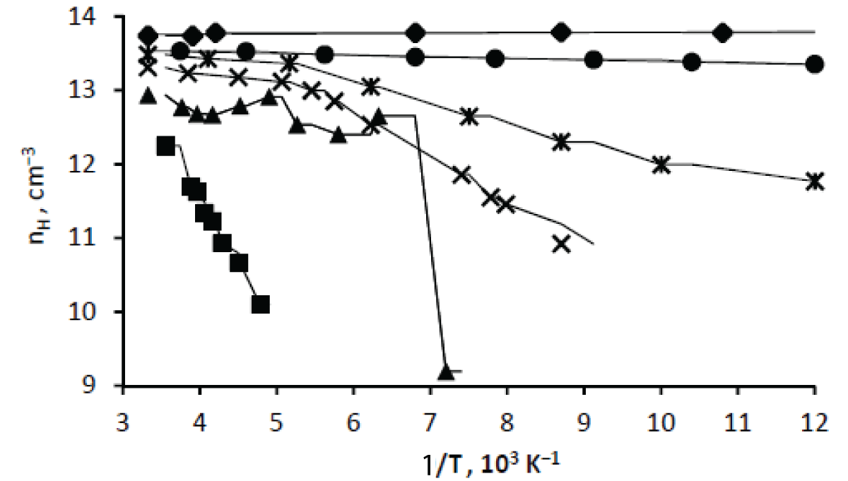
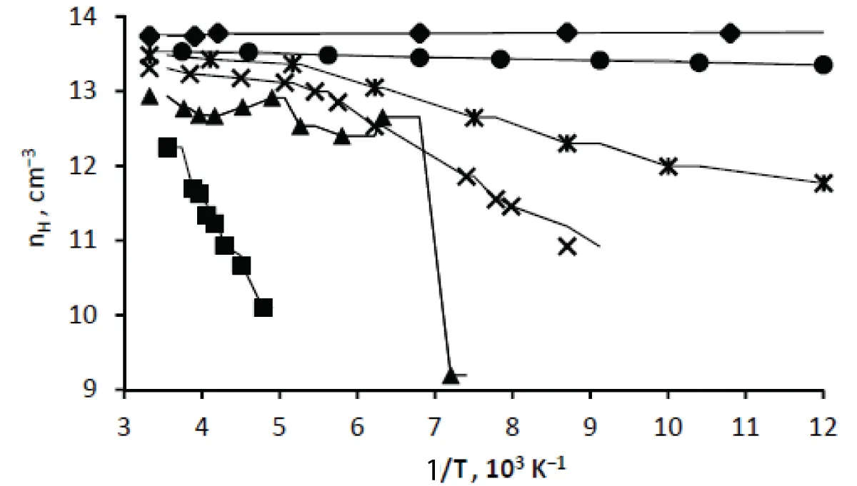
The obtained temperature-dependences of the electron Hall concentration are presented in Figure 1. Curve 1 corresponds to electron depletion of small donor centers of dopant phosphorus in the initial, i.e. non-irradiated, sample. The straightness (on the semi-logarithmic scale) of this dependence for the irradiated, but not annealed, sample (Curve 2) indicates the ionization of levels with an energy of around EC–0.36 eV.
Figure 1: Temperature-dependence of electrons Hall concentration in n-type silicon single crystal before irradiation (1 – •), after irradiation (2 – ■) and annealing at temperatures of 110 (3 – ▲), 120 (4 – ×), 290 (5 – ж) and 380 C (6 – ●).
Approximately the same value follows from the straight section, corresponding to the temperature range 130–150 K, of the nH – 1000/T dependence of same sample annealed at 110 °C (Curve 3). At higher temperatures, the general tendency for an increase in the electron concentration is retained, although its temperature dependence ceases to be monotonic: two minima appear on the corresponding curve in the vicinity of 177 and 244 K.
Such temperature-oscillations of the electron’s Hall concentration disappear after annealing the sample at 120 and 290 °C (Curves 4 and 5). After annealing at 380 °C, the electron’s Hall concentration again becomes almost independent of temperature (Curve 6), although its original value is not fully restored: it remains slightly lower than the value measured in the initial sample.
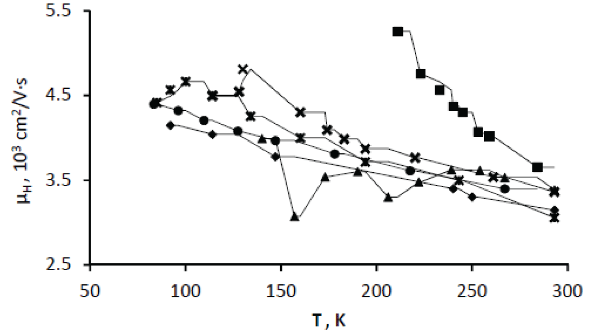
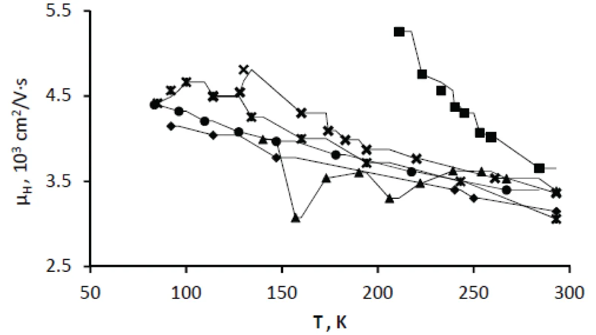
Figure 2 shows the measured temperature-dependences of the electron’s Hall mobility. Electrons Hall mobility in the initial, i.e. unirradiated, sample with good accuracy follows the 3/2-law:
Figure 2: Temperature-dependence of electrons Hall mobility in n-type silicon single crystal before irradiation (1 – •), after irradiation (2 – ■) and annealing at temperatures of 110 (3 – ▲), 120 (4 – ×), 290 (5 – ж) and 380 C (6 – ●).
(4)
(Curve 1). After irradiation, the temperature curve of the measured Hall mobility sharply shifts upward (Curve 2), and after sample annealing at 110 °C, the mobility values decrease again and two minima appear on the µH - T curve in the vicinity of 160 and 200 K (Curve 3).
The temperature-dependences of the electron’s Hall mobility in samples annealed at 120 and 290 °C are shifted upward and show maxima in the regions of 100 and 125 K, respectively (Curves 4 and 5). Finally, by annealing at 380 °C the µH - T dependence becomes monotonic and the mobility values measured in the initial sample at the same temperatures are approximately restored (Curve 6). Although the Hall mobility 3/2-temperature-dependence is now observed only on average.
Crystals of p-type silicon
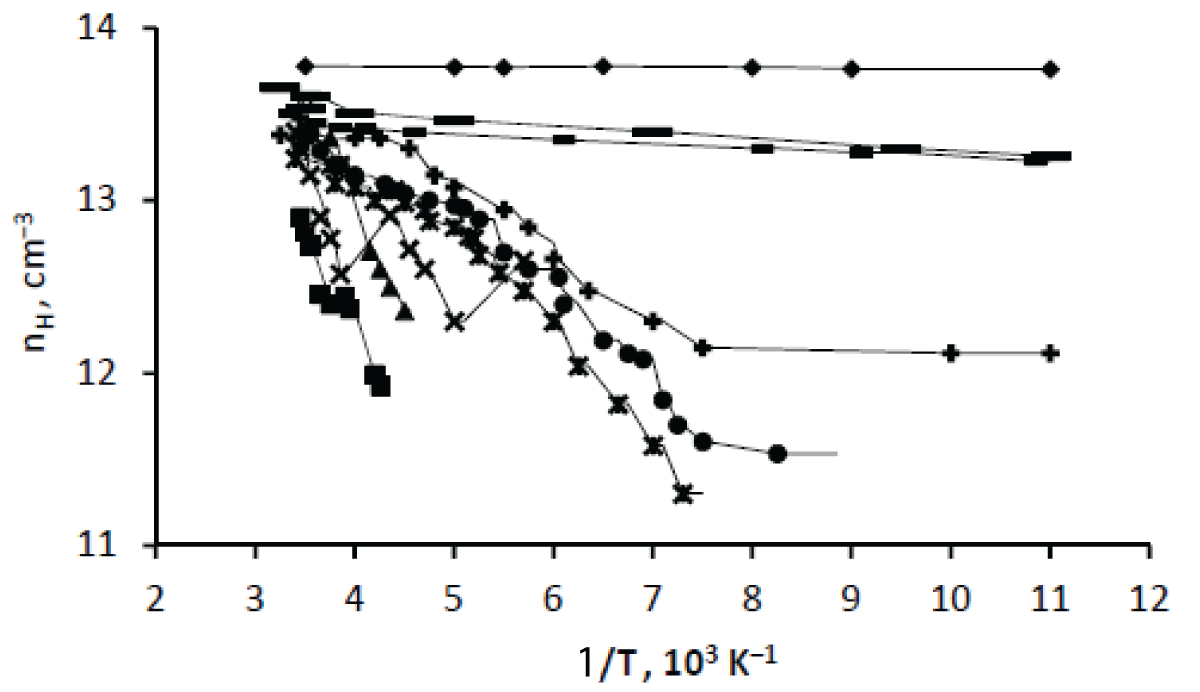
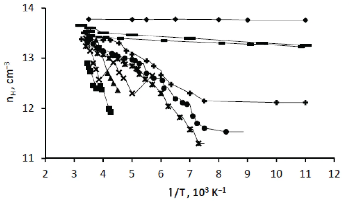
Figure 3 presents the measured temperature-dependences of the holes Hall concentration in irradiated single-crystalline p-type silicon. Curve 1 for the initial (non-irradiated) sample shows the constancy of hole concentration practically over the entire measurement range, and Curve 2 for the irradiated, but not annealed, sample shows the depletion of the acceptor level Ev+0.44 eV by holes.
Figure 3: Temperature-dependence of holes Hall concentration in p-type silicon single crystal before irradiation (1 – •), after irradiation (2 – ■) and annealing at temperatures of 80 (3 – ▲), 90 (4 – ×), 120 (5 – ж), 170 (6 – ●), 180 (7 – +), 360 (8 – –) and 500 С (9 – ▬).
According to Curve 3, in a sample annealed at 80 °C there are acceptor levels Ev+0.20 eV. In Curves 4, 5, 6, and 7 corresponding to annealing at 90, 120, 170, and 180 °C, one can identify parts indicating depletion of the acceptor level Ev+0.13 eV. Curves 8 and 9 corresponding to annealing at 360 and 500 °C, again show the practical constancy of the hole’s Hall concentration with temperature change.
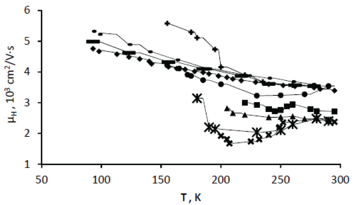
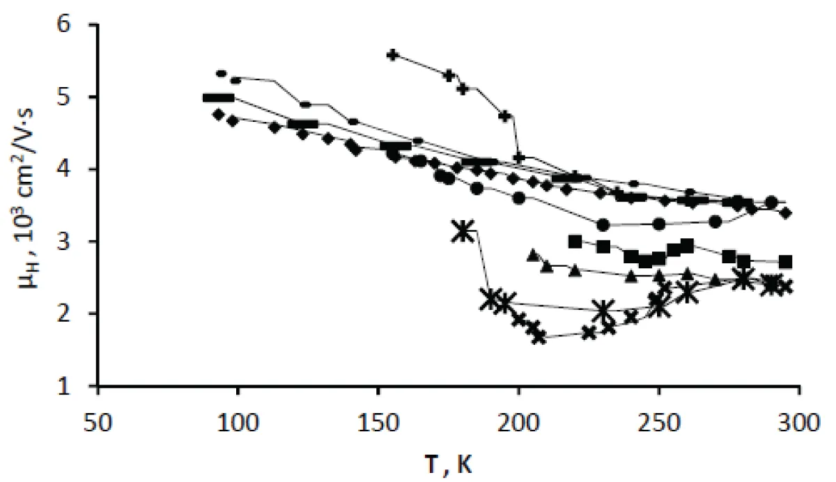
The temperature-dependence of holes Hall mobility in irradiated single-crystalline p-type silicon is shown in Figure 4. The temperature curve obtained for holes Hall mobility in unirradiated silicon (Curve 1) is typical of a pure phonon scattering mechanism. Curve 2 shows that in p-Si, in contrast to the case of n-Si, a sharp decrease in the Hall mobility of the charge carriers occurs immediately after the irradiation.
Figure 4: Temperature-dependence of holes Hall mobility in p-type silicon single crystal before irradiation (1 – •), after irradiation (2 – ■) and annealing at temperatures of 80 (3 – ▲), 90 (4 – ×), 120 (5 – ж), 170 (6 – ●), 180 (7 – +), 360 (8 – –) and 500 С (9 – ▬).
The effective Hall mobility of holes continues to decrease as a result of annealing at temperatures of 80 and 90 °C (Curves 3 and 4). However, after annealing at 120, 170, and 180 °C (Curves 5, 6, and 7), it begins to increase and the values of holes’ effective Hall mobility can even exceed those in unirradiated samples at the same temperatures. Annealing at 360 °C again leads to a decrease in the effective Hall mobility of holes (Curve 8), although its values still remain higher than in the unirradiated sample. Only by annealing at 500 °C is the original temperature dependence of the mobility completely restored (Curve 9).
Modelling
Models development: It is known that the decrease in the low-temperature Hall mobility µH of the majority of current carriers in silicon crystals irradiated by low-energy particles is due to the formation of charged point RDs, which serve as the most intense scattering centers of current carriers at low temperatures. As for irradiation with high-energy particles of the same types, at approximately equal concentrations of the same RDs the value of H decreases significantly more. Based on similar facts, Wertheim suggested [32] that in the initial n-type material, in addition to point RDs, the DRs with hole conductivity, i.e. inclusions of p-type silicon, also arise, the characteristic radius of which is comparable with the conduction electrons average wavelength. Of course, such formations separated from the matrix by p–n junctions would be not transparent for electrons and represent “dielectric” inclusions leading to a sharp decrease in H. On the other hand, to describe radical changes in the electrical properties of germanium, another elementary semiconductor with a diamond-like structure, after its irradiation with neutrons, Crawford & Clelend proposed [33] a cluster model, but noted that it is not able to explain a minimum appearance at the end of the Hall mobility temperature-dependence decreasing curve. An alternative description of the cluster model was almost simultaneously given by Gossik [34]: these clusters seem to be microscopic spheroidal inclusions containing high concentrations (1018–1020 cm–3) of defects capable of capturing the current carriers and, accordingly, are characterized by lower conductivity than the matrix undamaged by irradiation. Due to the charge carriers’ diffusion tending to equalize their concentrations in clusters and matrix, a cluster becomes charged and a spheroidal shell of opposite space charge formed around it depletes the charge carriers in the matrix at a certain distance from the cluster. In Gossik’s model, DRs influence the charge carriers’ mobility both geometrically and electrically: on the one hand, they simply block the flow of current carriers by reducing the effective cross-section of the sample and, on the other hand, the charged DRs serve for additional scattering centers.
Subsequently, it was suggested [35] that DRs in irradiated silicon would consist of cores with saturated multivacancy complexes and shells, in particular, containing complexes of monovacancies with impurity atoms. Such shells can be formed through the core monovacancies diffusion in the matrix, where they enter into quasi-chemical reactions with impurities. In this case, the depth of monovacancies penetration into the matrix and, therefore, the shell thickness is determined by the impurities concentration. The experimentally observed [36] downward shifts of the carrier mobility in temperature-dependence curves in differently doped n-type germanium samples with an increase in the dose of irradiation with 2.5 MeV electrons agreed well with the results of theoretical calculations based on the equation of electroneutrality of samples based on the RDs energy levels spectrum and taking into account the irradiation related changes in (1) charge states of multiply charged centers of RDs due to the Fermi level displacement; (2) concentrations and other parameters of scattering centers; and (3) scattering centers screening by charge carriers. The sharp fall in µH in the range of 240–180 K, detected [37] in n-Ge irradiated with electrons of 15 MeV energy, can be associated with the presence of barriers to electron drift along the electric field. However, the non-monotonic change in Hall mobility with decreasing temperature – first, the appearance of a deep minimum and then an increase in its value – as is noted, does not find a consistent explanation within the framework of such theories.
In [38], minima in the region of 100 K on the µH - T curves of phosphorus-doped n-Si single crystals (with an oxygen content of ≤1016), which were first irradiated with protons of energy 24 MeV and then electrons of energy 2.2 MeV, were attempted to be explained by the conduction electrons trapping on the electrically interacting centers (A- and E-centers, divacancies, etc.) in the DRs shells. According to this model, such centers are responsible for the anomalous scattering of electrons since an electron captured by some center after some time ∆τ(T) is again ejected into the conduction band. This leads to a decrease in the relaxation time τ(T) of the electron momentum in the irradiated sample compared to its value τ0(T) before irradiation:
. (5)
Here the temperature function f(T) is the degree of filling of the trapping centers. The value of ∆τ(T) increases with decreasing temperature, while f(T) decreases. This means that as the temperature decreases, the trapping effect decays. Reaching the limit τ(T) = 0 means the final capture of the electron, when it completely ceases to participate in conduction. In the trapping mode, the temperature function τ(T) can pass through a minimum, since the relaxation time τ0(T), as a rule, also increases with decreasing temperature, e.g. for purely phonon mechanism of scattering of electrons:
. (6)
Electron drift mobility µ is proportional to the average momentum relaxation time ⟨(T)⟩:
(7)
where e is the elementary charge and m is the effective conductivity mass of the electron. However, averaging over the conduction electrons energies leads to the appearance of a factor monotonically dependent on the temperature. Consequently, a minimum can be observed in the µH – T dependence as well.
The electron’s Hall mobility in P-doped silicon single crystals was measured [39] in the temperature range of 77–300 K in a series of samples both before and after irradiation with electrons or protons and thermal treatment. In the low-temperature region, the magnitude of µH significantly decreased with radiation dose. In some cases, one or two minima on the µH – T curves have been detected. The explanation was given by using the model based on the thermal polarization of the pairs of RDs.
There was constructed [40–43] a phenomenological theory of electron transport in a semiconductor with a nano-sized “metallic”, i.e. with higher than matrix conductivity, inclusions that can be screened by major carriers trapped on deep centers. In such heterogeneous samples, depending on the degree of screening the charge carriers’ effective Hall mobility can be either higher or lower than that in the semiconductor matrix itself. In the temperature region of lowered values, a minimum of the effective Hall mobility is expected.
If µm and µd denote the electron’s effective Hall mobilities, respectively, for the completely unscreened, i.e. ideally “metallic” (with infinite conductivity), and completely screened, i.e. ideally “dielectric” (with zero conductivity), inclusions in a semiconductor and µ is the electrons Hall mobility in the semiconducting matrix, one can write:
(8)
and
(9)
where
(10)
and
(11)
are some dimensionless coefficients always satisfying the condition:
(12)
These parameters are determined by factors such as total volume fractions of inclusions, their size, shape, and orientation relative to the electric current, interconnections between them, etc. dependent on the sample prehistory including its radiation- and thermal treatments.
For electron gas obeying the Boltzmann statistics, the probability of the absence of an electron on the dominant trap-level E at the temperature T is proportional to the exponent exp(-E/kT). Apparently, the probability wm that inclusions are unscreened, i.e. “metallic”, is proportional to the probability of the electron absence on the trap:
(13)
Here w is a temperature-independent coefficient. Its value is determined by the trap concentration in the screening shells, their mean thickness, and also external influences on the sample during the electrical measurements, e.g. IR illumination. Probability wd that these “metallic” inclusions are screened by their shells, i.e. act as “dielectrics”, is:
(14)
Effective Hall mobility can be expressed by weighted effective mobility in samples with ideally “metallic” and ideally “dielectric” inclusions:
(15)
or
(16)
To find its temperature dependence, one should take into account the charge carriers’ Hall mobility in the matrix. Within the phonon-scattering temperature range, this dependence is approximated by the decreasing exponential function
(17)
where
(18)
is the temperature-independent coefficient characterizing semiconducting material and
(19)
is the dimensionless exponent.
Explore the behavior of the
(20)
function, when the dominant trapping level is sufficiently deep to meet the condition
(21)
where Tmin is the minimum point determined by the transcendental equation
(22)
One finds that the expression
(23)
determines the ratio of the effective electron mobility in material with inclusions and electron mobility in the matrix at T = Tmin.
Based on formulated phenomenological theory, there were analyzed the experimental temperature-dependences of dark- photo-Hall effective mobilities of electrons and holes in n- and p-type silicon samples doped with P or B, respectively, irradiated at room temperature with significant doses of 25 MeV protons and/or 2–8 MeV electrons. The conclusion was made that irradiation-induced “metallic” inclusions screening in silicon should be related to vacancy complexes with background (oxygen) impurities and dopants. In n-Si, these are A-centers or V+O: Ec–0.17 and E-centers or V+P: Ec –0.44, while in p-Si these are V+B complexes: Ev +0.45 eV.
The distributions of RDs subcluster’s radii and distances between their cores were calculated [44] for Si (as well as GaAs, InGaAs, and GaN) samples and a burst in the hot electrons drift velocity before and after their neutron-irradiation was predicted. This effect should be sensitive to the presence of RDs clusters. The characteristic length, at which the burst effect manifests itself, amounts to 10–100 nm both before and after irradiation.
On the basis of the generalized effective field approximation, a formula was derived to calculate the effective dielectric characteristics of a matrix composite containing spherical inclusions of an insulating core with metal shells [45]. It can be considered a generalization of the classical Maxwell–Garnett formula for a matrix medium with inhomogeneous inclusions consisting of anisotropic cores and isotropic shells. It is shown that inclusions with metal shells in a matrix composite result in an additional plasmon resonance (compared to a composite containing all-metal inclusions) responsible for the material’s very low transmittance in the UV (UltraViolet) region.
The above-described theoretical model key idea – DRs formation in irradiated semiconductors – has received experimental confirmation as well.
It was found [46] that an anomalous decrease in the charge carriers Hall mobility in n-Si irradiated with fast neutrons appears only up to certain doses: ∼7·1014 n/cm2. A further increase in the irradiation flux leads to an increase in µH, but not higher than the initial value. These experimental results were explained by changes in the volumes of space charge regions around clusters in the form of shells of defects due to the introduction of isolated point defects during irradiation. Based on (photo-) Hall experiments, it was demonstrated [47,48] that in n- and p-Si samples irradiated with protons of energies of 30 and 640 MeV, respectively, and fast neutrons the shells of DRs actually consist of secondary RDs: A- (complex of a background oxygen impurity with a vacancy OV) and E-centers (donor, usually phosphorus, complex with a vacancy PV), BV (boron–vacancy complex), etc. As for cores, in addition to multivacancy complexes, they must also contain interstitial atoms and their associates. And their sizes depend on the irradiating particles’ energy.
DLTS (Deep Level Transient Spectroscopy) studies of n-type silicon at room temperature implanted with low doses of 5.6 MeV Si ions and later annealed show [49] that the divacancy V2 and oxygen-vacancy OV centers produced after ion implantation disappear at lower temperatures compared to electrons-irradiated high purity material. This is mainly attributed to the fact that MeV ion implantation results in the formation of a non-uniform defect distribution and hence enhances diffusion of point defects until they are annihilated through quasi-chemical reactions with traps in the implanted material, e.g. interstitial O, substitutional C, and H atoms, and/or localized DRs.
A significant growth of luminescence observed in proton-irradiated silicon was attributed [50,51] to the formation of special rod-shaped clusters of interstitial-type radiation defects. Sequential implantation of 100, 200, and 300 keV protons with equal flounces causes the formation of µm-thick damaged layer, which forms simultaneously with intrinsic clusters of vacancy- and interstitial-type RDs. Vacuum annealing of the irradiated crystals at 600 C increases the effect of RDs of both types despite reducing their concentrations. Interstitial-type RDs dominate after annealing at 1100 °C. The excess carrier lifetime distribution in multicrystalline silicon should be caused [52] by the electrical activity of extended defects – grain boundaries, dislocations, and impurity microinclusions.
Qualitative model construction and verification: The upper limit of the energy ε of interaction between deeply charged centers in a semiconductor can be estimated as
(24)
at
(25)
where η is the degree of their filling (see, e.g. [53]). Here e is the electron charge, ε is the semiconductor dielectric constant, d is the average distance between the defects forming such centers, and ε0≈8.85·10–12 F/m is the electrical constant. Let us analyze the experimental results obtained above regarding the effect of irradiation with high-energy particles and isochronous annealing cycles on the temperature dependence of conduction electrons concentration in silicon in light of the possibility of a significant electrostatic interaction between charged radiation defects.
Irradiation of n-Si with high-energy protons leads to an increase in the share of electrostatically interacting centers (A- and E-centers, divacancies, etc.) since it creates primary RDs along the proton paths capable of condensing into nearby vacancy complexes and DRs clusters. According to our estimates, the distances d between electrostatically interacting RDs along these tracks are around 10–7 cm, and η tends to be 1. Since the dielectric constant of silicon is ε≈11.7, it turns out that ε>max0.1 eV. This is a significant value that can influence the ionization energies of centers. It should be taken into account that in n-Si, in addition to negatively charged deep acceptors, there are also positively charged shallow donors. The deviations (increase or decrease) in the ionization energies of point centers in irradiated silicon were indeed observed.
The nH-1000/T dependence for the initial sample (Figure 1, Curve 1) shows that throughout the entire temperature range of measurements, the dopant small donors are depleted of electrons. This corresponds to the constancy of their concentration. But, during irradiation, RDs and DRs are formed relatively uniformly along the proton paths. In this case, the DRs presented in the crystal create the elastic stresses. When irradiated samples are annealed, monovacancies and decay products of secondary RDs with relatively low thermal stability tend to the DRs and, in their vicinity, enter into quasi-chemical reactions with impurity atoms. As a result, point RDs with high concentration are formed around the DRs, which leads to an increase in the energy of electrostatic interaction between them.
The detected oscillation of the electron’s Hall concentration value at a fixed temperature depending on the irradiation temperature can be explained by the electrostatic interaction between charged secondary point RDs (A- and E-centers, divacancies, etc.) located around nano-sized DRs. The electron bounding energy at i-center is approximately expressed by the sum
(26)
where Ei is its value in the absence of electrostatic interaction with other charged centers, which is practically independent of temperature. In particular, silicon, its weak temperature dependence is monotonic (namely, increasing). As for ε(T), this term depends on the degrees of filling of A- and E-centers and divacancies with electrons and, therefore, changes non-monotonically with temperature.
Elastic stresses created in the crystal by DRs reduce the annealing temperature of vacancy-type defects such as E-centers and tetravacancies V4 [54]. During the annealing process at 110 °C, nonequilibrium vacancies, E-centers, and tetravacancies decay-products tend to the DRs and enter into quasi-chemical reactions with impurity atoms, which leads to an increase in the concentration of electrostatically interacting point defects around them.
Annealing of irradiated samples at 110 °C leads to the appearance of two temperature-minima, at 177 and 244 K, in the electron concentration (Figure 1, Curve 3). After annealing of E-centers and divacancies V2, respectively, at 120 and 290 °C, the electron Hall concentration monotonically increases with temperature (Figure 1, Curves 4 and 5). The fact, that even after final annealing at 380 °C (Figure 1, Curve 6) the initial electrons Hall concentration is not completely restored, indicates that some of the phosphorus dopant atoms remain bound in E-centers (EC–0.17 eV) and, perhaps, DRs.
The level of Ec –0.36 eV detected in the irradiated sample appears to be a hybrid one – arising from the levels of electrostatically interacting charged centers A–, V2– –, V2– and E– with levels of EC–0.17, 0.21, 0.39 and 0.44 eV, respectively. Since they are all negatively charged, their interaction should lead to a decrease in the corresponding deionization energies through transitions of captured electrons to the conduction band and, therefore, the effective increase in the Hall concentration of quasi-free electrons compared to their equilibrium Hall concentration at a given temperature. We emphasize that here by the term “equilibrium” we mean the state of the semiconductor electronic system when the charged centers’ spatial distribution is such that the electrostatic interaction between them is negligible.
As the temperature rises A–-center-related levels, the shallowest among deep energy levels, should be the first to be depleted of electrons. Their deionization leads not only to an increase in the electron’s Hall concentration but also to a weakening of the electrostatic effect on the remaining ionized centers, thereby effectively increasing their ionization energies. As a result, the effective Hall concentration of electrons in the conduction band decreases. The competition of these two mechanisms leads to the appearance of the first minimum at 177 K. Similarly, i.e. by the depletion of the next shallower level of the doubly charged divacancy, it can be explained the appearance of the second minimum at 244 K in the electrons Hall concentration temperature-dependence. Note that in this case, the charge of the defect center does not completely disappear, but only decreases, since doubly negatively charged divacancies turn into singly charged ones.
The limitation of the measurements region to room temperature does not allow us to determine whether higher temperature minima, associated with electron depletion of the deeper V2– and E– levels, exist or not. With regard to E-centers, it should also be noted that, unlike A-centers and divacancies, in the temperature range of measurements, in the main part they do not change the charge state and, thus, always contribute to the electrostatic interaction of charged centers.
Now let us consider the effect of irradiation directly on the electron Hall mobility in silicon. As noted above, the average relaxation time of electron momentum during its purely phonon scattering is ∽1/T . On the other hand, the energy-average thermal velocity of electrons, at their Boltzmann energy distribution, is ∽1/T1/2. Therefore, the mobility, which is proportional to the electron momentum relaxation time averaged over their energies, precisely leads to the ∽1/T3/2 law. We come to the conclusion that in the unirradiated sample, throughout the entire temperature range of the conducted measurements, the phonon mechanism of electron scattering prevails over the impurity one.
Of course, irradiation of a semiconductor with high doses of high-energy particles multiplying defects should lead to a decrease, not an increase, in the drift mobility of current carriers. However, according to the effective medium theory of galvanomagnetic phenomena [55], the apparent or measured Hall mobility – let us call it the effective mobility µeff – can indeed significantly exceed the real drift mobility if the semiconductor contains sufficiently highly conductive, compared to the matrix, and sufficiently voluminous inclusions. Attention to the possibility of this effect in irradiated silicon was first drawn in [56]. Further studies [57–61] supported the formation of high-conductive, i.e. “metallic”, inclusions with Ohmic interfaces with a matrix of irradiated silicon. In certain conditions, they can convert it into low-conductive, i.e. “dielectric”, inclusions due to their screening by charged defects.
Namely, an increase in the value of µeff in irradiated silicon is associated with the formation of nanosized DRs in the form of accumulations of intrinsic and dopant interstitial atoms. These excess atoms can occupy adjacent interstitials and thus be interconnected like regular atoms in a silicon crystal. Essentially, such clusters are nanocrystals placed in a single-crystal matrix [62]. Their high conductivity is associated with the high concentration of dopant atoms in them. Let us estimate the total volume fraction p and the size R of highly conductive DRs in the measured n-Si samples. Assuming that the DRs shape is spheroidal, Hall µH and effective µeff mobilities are related by the formula
(27)
whence
(28)
According to Curves 1 and 2 of the Figure 2, µH≈1400 and µeff≈4500 cm2/V·s. By substituting these values in the above relation we get p≈0.10.
Thus, the total volume fraction of inclusions in silicon irradiated with high-energy particles can be estimated from the temperature dependence of charge carriers’ Hall mobility. However, the data obtained by Hall measurements are insufficient for the estimation of the formation probabilities of these
large-scale defects. As for the concentration of primary radiation defects, they can be estimated as the ratio of irradiation dose and depth of particle penetration.
Depths of penetration of protons of given energy (25 MeV) in n-Si were determined for samples of special form by measuring their electrical resistivity at several different doses. The linear extrapolation of the results to the applied dose of 8.1·1012 cm–2 yielded a value of 0.37 cm well coincided with that yielded from the linear extrapolation of the energy-dependence recommended [63] in the literature for the depth of proton penetration in silicon. The above-estimated value of the penetration depth of 25 MeV protons is supported by the earlier experimental data as well [64–67]. So, there are expected dose/depth = 8.1·1012/0.37 ≈ 2.2·1013 cm–3 primary defects in the proton-irradiated silicon. Because of their heaviness, high-energy protons can directly create primary defects in the form of DRs.
The available data evidence of the dominance of elastic scattering of high-energy (≥25 MeV) protons in silicon. However, this does not mean that the probability of the appearance of the recoil atom with the energy, which would have been enough for creating a disordered region or a cluster of structural point defects in the crystal subjected to irradiation with 25 MeV protons, is small. The point is that, according to the review on displacement damage effects in silicon [68], e.g. for a 20 MeV proton the recoil energy is estimated to be only 12–20 keV. As the proton energy significantly exceeds the recoil energy, every act of high-energy proton scattering by the silicon lattice seems to be almost elastic. However, in their turn recoil energy in silicon significantly exceeds atoms displacement energy, i.e. energy of vacancy–interstitial (Frenkel) pair formation, which equals only 13 eV [69]. It is the reason why at high proton energies, it takes place the many sub-cascade scatterings accompanied by the formation of a high number of Frenkel pairs.
If the parameter R has the meaning of the average radius of a spheroidal inclusion, and v is the concentration of such inclusions in the sample, then the average volume per inclusion can be expressed in two ways:
(29)
whence
(30)
In our experiment, v≈5.0·1013 cm–3 and, therefore, R≈78 nm. Thus, DRs are truly nanosized.
Highly conductive inclusions, on the one hand, increase the effective mobility of electrons in the sample as a whole, but, on the other hand, reduce their Hall mobility in the matrix. This effect can be modeled as a Coulomb blockade by a charged conductor. The electrical capacitance C of a conductive spheroidal inclusion of radius R is equal to
(31)
where ε is the dielectric constant of the media, i.e. semiconductor. For R≈78 nm and ε≈11.7, which correspond to our experiment, we obtain C≈1.01·10–16 F. The potential ϕ of a spheroidal conductor with charge q is equal to
(32).
If such a cluster captures at least one electron or hole, i.e. has an elementary charge q = e, then its potential reaches a value of ∼0.002 V, which seems to be sufficient for Coulomb blocking of current carriers.
The decrease in the electron’s effective Hall mobility in samples annealed at 110 °C (Figure 2, Curve 3) can be explained by the appearance of a defective shell around highly conductive inclusions. Namely, at 110 °C, secondary RDs with low thermal stability, including some E-centers, are annealed. The products of their decay and other nonequilibrium vacancies tend to the DRs, enter into quasi-chemical reactions there, and form shells that contain increased concentrations of A- and E-centers, divacancies, etc. At sufficiently low temperatures, they are all negatively charged (most divacancies are doubly negatively charged) and therefore interact strongly electrostatically.
With increasing temperature, the shallower levels created by A-centers and singly charged divacancies V2– are first deionized, the scattering of electrons by them becomes significantly weaker, and, consequently, the mobility increases. At the same time, the electrostatic interaction between charged defect centers weakens, which leads to an increase in the depth of the corresponding energy levels and, thus, a slowdown in their deionization. As a result of the competition of these two mechanisms at a certain temperature, the increase in mobility changes to its decrease. The appearance of the first mobility minimum at 100 K is associated with the onset of deionization of deeper levels, such as E-centers and doubly charged divacancies V2– –, and associated increase in mobility. However, with a further increase in temperature, the competition of this process with the accompanying weakening of electrostatic interaction and deionization again leads to the replacement of the increase in mobility with its decrease. The mobility second minimum in the region of 200 K is associated with the dominance of the phonon scattering mechanism over the impurity one at sufficiently high temperatures.
After complete annealing of E-centers at 120 °C (Figure 2, Curve 4), divacancies remain. While most of them are doubly charged, the electron’s effective Hall mobility increases with temperature and reaches its maximum in the region of 130 K. Now most of the divacancies are singly charged and due to their small concentration (1·1013 cm–3) are not able to completely screen highly conductive DRs, i.e. transform them into “dielectric” inclusions. Therefore, effective mobility begins to fall sharply with a further increase in temperature. After annealing divacancies at 290 °C (Figure 2, Curve 5), the effective mobility increases in the region of charged A-centers, and decreases above 100 K. Thus, the non-monotonicity of the temperature-dependences of the electron’s effective Hall mobility in samples annealed at 120 and 290 °C (Figure 2, Curves 4 and 5) is explained by changes in the DRs potentials with temperature, which in turn are determined by the degrees of filling of the RDs in their shells and the electrostatic interaction between them.
Deviations of both signs of the µH-T dependence of the sample annealed at 380 °C (Figure 2, Curve 6) from the µH∽T3/2 law indicates the presence of traces of unannealed highly conductive DRs, which, however, do not have sufficient electrical potentials for Coulomb blockade, since there are practically annealed all RDs (A- and E-centers and V2 divacancies) in their shells.
Figure 3, Curve 1 of the holes concentration temperature-dependence in the initial sample corresponds to the depletion of small acceptor levels of dopant boron atoms in p-Si. In regard to Figure 3, Curve 2 of the irradiated sample indicates the presence of acceptor level Ev+0.44 eV, it should be noted that a close value of the level Ev +0.45 eV is characteristic of the complex of dopant boron atom with vacancy BV, which is annealed only in the region of 200 °C [70,71]. Such identification of the detected level seems to be quite reliable if we take into account the possibility of deviations of discrete electron/hole levels in the irradiated semiconductor due to significant electrostatic interaction between charged defects in the DR’s shells. Figure 3, Curves 3, 4, 5, 6, and 7 for samples annealed, respectively, at temperatures of 80, 90, 120, 170, and 180 °C indicate the presence of a number of other acceptor centers in irradiated p-type silicon. For two of them, the locations of energy levels have been established: Ev+0.13 and 0.20 eV.
Figure 3, Curves 8 and 9 for samples annealed at temperatures of 360 and 500 °C, respectively, reflect the transition of electrons from the valence band to shallow acceptor levels of dopant boron atoms. In this case, the hole’s initial Hall concentration is not completely restored: apparently, some boron atoms remain bound in ВV complexes and other point RDs, as well as DRs. Annealing of all RDs in p-Si occurs only at 600 °C.
The observed excess of the hole’s effective Hall mobility measured in irradiated samples annealed at 180 and 360 °C (Figure 4, Curves 7 and 8) over their Hall mobility before irradiation is again explained only by the presence of highly conductive inclusions. The mobilities at room temperature, determined from Figure 4, Curves 1 and 7, respectively, are equal to µH≈2500 and µeff≈3500 cm2/V·s, and for the total volume fraction of these inclusions in the sample annealed at 180 °C we obtain p≈0.035.
Approximately, the depth d of electron penetration in solids can be calculated by the formula [72]:
(33)
where E is the mean energy of electrons in the beam and ρ is the density of the material. For silicon, ρ≈2.33 g/cm3, irradiated with E=8 MeV electrons we get d≈0.0031 cm. So, at the dose of 5.0·1015 cm–2 there are expected 5.0·1015/0.0031 ≈ 1.6·1018 primary RDs per cm3 in the p-Si sample. Because of the lightness of electrons, almost all of them are point structural defects. So, for electrons-irradiated samples, we can estimate only the lower limit of created DRs average radius: R>5 nm.
A decrease in the hole’s effective Hall mobility after irradiation and annealing at different temperatures (Figure 4, Curves 2, 3, 4, 5, and 6) can be associated with Coulomb blockade caused by the presence of charged RDs, for example, boron–vacancy complexes that have captured holes BV+, the presence of which is confirmed by analysis of the temperature-dependences of the holes Hall concentration in tested samples. These and other charged RDs, which revealed in the holes Hall concentration and mobility temperature-dependences non-monotonicity, have to form the defective shells around the RDs. In this context, the upward shift of the µeff-T curve (Figure 4, Curve 7) is explained by the annealing of the ВV+ complexes at 180 °C and the subsequent drop in the scattering potential of the DRs. First partial and then complete restoration of the initial mobility after annealing at 360 and 500 °C (Figure 4, Curves 8 and 9) indicate that scattering by the remaining unannealed RDs is small or completely negligible compared to phonon scattering.
Summarizing and generalizing the results of the study carried out on the single-crystalline silicon, a qualitative model of the mechanism of electrical conductivity of a semiconductor irradiated with high-energy particles can be represented as follows:
– Irradiation of a semiconductor with sufficiently high doses of sufficiently high-energy particles and its annealing at a certain temperature, in addition to primary (nonequilibrium vacancies and interstitials) and secondary (complexes of vacancies and interstitials between themselves and dopant and background impurities) point radiation defects, leads to the formation of nano-sized inclusions in the form disordered regions.
– In certain temperature ranges, inclusions of disordered regions can be highly conductive, compared to the semiconductor matrix, and separated from it by Ohmic junctions. In particular, in irradiated silicon highly conductive inclusions appear as clusters of highly doped nanocrystals. Hall measurements of the electrical-physical parameters of a semiconductor containing a fairly high total volume fraction of highly conductive inclusions lead to the effective value of the majority of current carriers' Hall mobility, which significantly exceeds the corresponding value of the Hall mobility in the semiconductor matrix.
– Due to elastic stresses created by inclusions of disordered regions, from the matrix the high concentrations of point radiation defects tend to them, as cores, enter into quasi-chemical reactions with each other and impurities, and form the defective shells around them. In particular, irradiated silicon shells of highly conductive inclusions contain nonequilibrium vacancies V, divacancies V2 and tetravacancies V4, A- and E-centers, BV complexes, etc. In certain temperature ranges, such nanosized core-shell structures can have electric charges sufficient for the Coulomb blockade of the major charge carriers. In particular, in irradiated silicon boron–vacancy complexes captured holes BV+ can act as charge capacitors. This transformation of highly conductive inclusions into low-conductivity ones manifests itself in a noticeable decrease in effective mobility.
Pagava T, Chkhartishvili L, Beridze M, Khocholava D, Shogiradze M, Esiava R. Qualitative Model of Electrical Conductivity of Irradiated Semiconductor. IgMin Res. April 12, 2024; 2(4): 199-212. IgMin ID: igmin166; DOI: 10.61927/igmin166; Available at: igmin.link/p166
Address Correspondence: Levan Chkhartishvili, Department of Engineering Physics, Georgian Technical University, 77 Merab Kostava Avenue, Tbilisi, 0160, Georgia, Email: [email protected]
How to cite this article: Pagava T, Chkhartishvili L, Beridze M, Khocholava D, Shogiradze M, Esiava R. Qualitative Model of Electrical Conductivity of Irradiated Semiconductor. IgMin Res. April 12, 2024; 2(4): 199-212. IgMin ID: igmin166; DOI: 10.61927/igmin166; Available at: igmin.link/p166


 Scan and get link