IGMIN: We're glad you're here. Please click 'create a new query' if you are a new visitor to our website and need further information from us.
If you are already a member of our network and need to keep track of any developments regarding a question you have already submitted, click 'take me to my Query.'
Welcome to IgMin Research – an Open Access journal uniting Biology, Medicine, and Engineering. We’re dedicated to advancing global knowledge and fostering collaboration across scientific fields.
At IgMin Research, we bridge the frontiers of Biology, Medicine, and Engineering to foster interdisciplinary innovation. Our expanded scope now embraces a wide spectrum of scientific disciplines, empowering global researchers to explore, contribute, and collaborate through open access.
Welcome to IgMin, a leading platform dedicated to enhancing knowledge dissemination and professional growth across multiple fields of science, technology, and the humanities. We believe in the power of open access, collaboration, and innovation. Our goal is to provide individuals and organizations with the tools they need to succeed in the global knowledge economy.
IgMin Publications Inc., Suite 102, West Hartford, CT - 06110, USA
In this paper we present a physics-based model for hot carrier surface mobility in semiconductor devices and sensors which incorporates the band structure and interface/surface effects. This model can be utilized within the generalized hydrodynamic model (HDM), for semiconductor device and sensor simulation [1]. The proposed non-local surface mobility model is essentially needed in the hydrodynamic transport modelling of hot carriers as an energy-dependent model. Unfortunately, most of the involved parameters in the hydrodynamic simulation of semiconductor devices and sensors are obtained from Monte Carlo simulation in the bulk of a homogenous semiconductor. However, the correct simulation of the dynamic behaviors of hot carrier transport across semiconductor surfaces and junctions, needs to consider the main variable gradients, such as the carrier density, energy (or temperature) and velocity gradients. In particular, the velocity gradient plays a significant role in the transport of hot carriers in 2D electron/hole gas devices. Therefore, our mobility model focuses on the role of velocity gradients of hot carriers and the Underlying carrier gas viscosity, to interpret the well-known surface mobility reduction, near the Si/SiO2 interface in nano devices and nano sensors. Unlike previous surface mobility models, which are primarily based on the local electric field and fitting of experimental data, our model is physics-based on the hot carrier energy and velocity gradients. Therefore, our model is also considered truly non-local and fully hydrodynamic.
It is taken for granted that the approach of the isothermal drift-diffusion model (DDM) is not adequate for the simulation of hot-carrier transport in semiconductor devices [1]. Therefore, researchers resorted to the fundamental theories of nonlinear transport in semiconductors [2]. There are two basic alternatives, namely, the semi-classical Boltzmann transport equation (BTE) and the quantum transport approaches, such as the non-equilibrium Green’s function (NEGF) and the Wigner-Boltzmann transport equation (WBTE) [3-6]. In addition to these microscopic approaches, one can add the macroscopic hydrodynamic moments of the BTE or the WBTE [6].
The formalism of the microscopic quantum transport theory, though rigorous for the nano-scale devices, but unfortunately is conceptually complicated and mathematically Unmanageable [3,4]. On a relatively large time and length scales (down to the 100nm range), the theoretical basis for high field transport has been mainly the BTE [5]. Several methods have been developed to solve this complicated equation [6]. Among the direct approaches, the Monte Carlo particle simulation (MC) has been the most successful [7]. However, particle simulation is extremely demanding on computational resources, and unsuitable for treating regions with potential barriers (e.g., p-n junctions and MOS interfaces), and low-field regions of substantial extent [8].
Other widely accepted technique to solve the nonlinear transport problems is based on the first moments of the BTE or the WBTE [9]. The moment approach is usually referred to as the hydrodynamic models (HDM). The so-called energy transport model (ETM) is a reduced version of the HDM. Such macroscopic nonlinear transport models trade between the DDM and the direct methods to solve the BTE or the WBTE. Therefore, the HDM is still used in the electronic industry and the academia to develop a wide range of semiconductor devices. However, the existing HDM-based device simulators are in short of accurate energy-dependent models of their physical parameters, such as the surface drift mobility of charge carriers. In this paper we derive a physics-based drift mobility model for hydrodynamic simulation of semiconductor devices, including band structure and surface effects. The surface effects on the hot carrier mobility are included via the velocity gradient terms of charge carriers, which come from the divergence of the tensorial product of carrier velocity and convective terms.
The paper is organized in five sections, an Appendix and a list of references, as follows. The first section is an introduction. In section II, we present the set of adopted hydrodynamic equations (HDE’s). In section III, we present the new mobility model, which is derived from the set of HDE’s in the Appendix. In section IV we present and discus some verification results. Finally, we present our conclusions in section V.
II. Hydrodynamic Model for Semiconductors, with Arbitrary Band Structure
The hydrodynamic model consists of the first moments of the BTET, which represent the conservation (continuity) equations of some physical quantities, such as the carrier average density, average momentum and average energy. In the adopted HDM, we content ourselves with the first three moments of the BTE for semiconductors with arbitrary band structure. For the matter of simplicity, we’ll only present the set of moment equations for a gas of electrons, which are suitable for monopolar devices, such as n-channel MOSFETs. A similar set of moment equations, for the gas of holes, should be added for the case of bipolar devices. Of course, the complete set of moment equations should be coupled with Poisson’s equation and solved, all together, to get the characteristics of any semiconductor device.
i - System of Hydrodynamic Equations (HDE’s)
The adopted set of semi-classical hydrodynamic equations for the gas of electrons, in a semiconductor, with arbitrary band structure, consist of the following continuity equations [10]:
(1a)
(1b)
∂
(1c)
where e is the electron elementary charge, n is the conduction electron density, vn, = <Un> is their average velocity, ωn = <En> is their average energy, and Pne is the electron gas electro-kinetic pressure tensor. By definition, is a second-order central moment, such that:
, where
is the sign of tensorial product and the angular brackets denote the statistical average over the electron distribution function in the wave-vector k-space
. Also, the electron current density (Jn) and energy flux (Sn) can be expanded from their basic definitions (
), as we’ll see later on. The average collision terms, denoted by [..]col., at the right-hand side of the three moment equations (1a), (1b), (1c) will be also expand in the following sections about the system closure. Finally, mn is the average mass tensor of conduction électrons, whose inverse components are defined as follows:
(1d)
This macroscopic mass quantity is measurable (e.g., by the Cyclotron Resonance or the Femtosecond Pump-Probe Reflectivity [11]) and can be also expressed as a function of the electron mean energy [1]. The electric field ζ = -∇ϕ, where ϕ is the electric potential, can be obtained by the aide of Poisson's equation [12]. In magnetic sensors, the magnetic field effects can be incorporated by replacing ζ → ζ _+ vnxB, where B is the magnetic field intensity.
ii. System closure
The above set of generalized HDE’s should be supplemented with some closure conditions, to be solved. The closure conditions usually make use of certain approximations, because some terms require the knowledge of the unknown distribution function,
. For instance the collision terms (
) as well as the high-order fluxes (such as Sn). In addition, we need to relate the electro-kinetic pressure tensor (Pne) to the average electron energy (wn). This relation can be established by relating both of them to the electon temperature (Tn).
1. Collision terms
To deterrmine the collision term in the conservation equation of average electron energy (1c), we adopt the energy-relaxation time approximation [13]. Therefore:
(2a)
where τU+A7B6n is the macroscopic energy-relaxation time of electrons, U+A7B6,sub>o is the average electron energy at thermal equilibrium (
), kB is the Boltzann constant and TL is the semiconductor lattice temperature. Also, (R-G) is the net recombination-generation rate. The later term is often neglected, because the energy relaxation time is usually much smaller than the carrier lifetime between generation and recombination events (τꞷn << τn).
The momentum collision term can be also replaced by a mobility term (µn), which is directly related to the electron scattering mechanisms, as explained in the Appendix A. Therefore, the electron mobility is defined as follows:
(2b)
Consequently, the electron momentum conservation equation, can be used to derive an expression for the electron current density (
), in steady state, as follows:
(3a)
This constitutive relation can be further expanded, after relating the electron gas pressure to the electronic temperature. Therefore, the hydrodynamic current density of carriers contains both drift and diffusion terms. In addition, the last term reflects the spacial acceleration/deceleration of carriers aroUnd the semiconductor interface regions and the viscocity near the surface. This term can be expanded as follow;
(3b)
The later term (∇.(n vn)) is equal to the net generation-recombination rate (G-R), which is often neglected, because the momentum relaxation time is much smaller than the carrier lifetime between generation and recombination events (τmn < erm is always dropped in unipolar devices such as MOSFETs. τn). Also this t Therefore;
(3c)
2. Expanding the high-order flux terms
The energy flux of electrons can be expanded from its basic definition ( Sn = <Enun>), as follows:
(4a)
Here, wn = <En> according to its basic definition, and Qn is the electron heat flux, which is defined as the third-order central moment of the distribution function.
(4b)
As the electron distribution function is not known, we’d resort to an approximate relation of Qn to close the system of HDE’s. Although the Fourier law for heat flux (
, where Tn is the temperature of electrons and knth is their thermal conductivity) is usually used in the literatature [22], a better model of Qn can be found in [14].
3. Expandingv the gas pressure
The electron gas pressure tensor (
) also depends on the distribution function, and needs to a certain approximation. According to the ideal gas theory, the electron gas pressure can be reduced to a scalar quantity (
) such that:
(4c)
4. Expanding the electro-kinetic gas pressure
For the matter of completing the closure of the system of HDE’s, we need to find an approximate expression for the electro-kinetic pressure
, which appears in momentum conservation (1b) and the current density constitutive relation (3c). Therefore, we need to relate Pne with either the average electron energy (ωn) or temperature (Tn). As the electro-kinetic pressure of a gas is a sort of gas pressure per unit mass, we can assume the following relation between Pne and Pn which is already related to the electron temperature by the ideal gas law (
).
, (5a)
where mn-1 is the average inverse mass tensor of électrons, as defined by (1d). Note that this approximation coincides with the ideal gas theory, where the gas pressure is usually defined as
, and the gas mass density rn = n mn is wave-vector-independent (macroscopic quantity) and can be taken outside angular brackets. However, the old-style definition of the gas pressure tensor
, involves the electron effective mass
is wave-vector dependent. Therefore, the above approximation can be improved by adding a correction factor (gn) as follows:
(5b)
The correction parameter can be calculated by Monte Carlo simulation in the bulk of a semiconductor. It can be reduced to a scalar value and modelled as function of the electon energy or temperature (
). Finally, we can substitute (
) in the current density
(5c)
Because the amount of added accuracy of final results by this correction factor, it may be considered a user-defined option in the simulation process (with default value gn-1).
iii. Quantum correctiions
In the so-called quantum hydrodynamics model (QHDM), both ωn and Tn are appended by an additional density gradient (DG) correction term [15]:
(6a)
where Vq is sometimes called the quantum (or Wigner) potential, and given by [16]:
(6b)
The so-called quantum electron temperature (Tqn) is related to the semiclassical electron temperature (Tn) by the following relation:
(6c)
The quantum correction appears also in the current equation, which is a reduced form of the momentum conservation equation (1b), in the form of an additional quantum current Jnq:
(6d)
with
(6e)
Note that the quantum correction term is only significant when the electron concentration n varies rapidly over small distances in the order of de-Broglie wavelength [1]. The DG method can correctly predict the carrier concentration in the inversion layer of MOSFET devices but fails to reproduce the tUnneling currents [17,18].
III. Surface mobility models
In this section focus on the modelling of drift mobility of mobile charge carrier (electrons and holes) and the surface mobility models, in particular. We consider the total electron drift mobility, due to all scattering mechanisms, in the parallel form:
, where mno is the low-field mobility, mnB is the hot-carrier mobility (due to parallel fields), and mns is the surface mobility (due to surface effects and normal fields).The normal electric field, near the surface of a semiconductor of an n-channel MOSFET devices pulls electrons closer to the gate interface. This leads to a decrease in the electron drift mobility not seen in the bulk. The so-called universal surface mobility models are used in the numerical simulation of MOSFET devices [19]. Besides, they are often used to evaluate the performance of new technology nodes of CMOS technology. However, the extensive studies showed that the universal surface mobility plots are affected by the semiconductor band structure [20]. In fact, the semiconductor devices usually have several interfaces to conductors or other semi-conductors (heterojunctions). The semiconductor surfaces and interfaces are not just like the bulk, where the semiconductor crystal periodicity is maintained. In addition, the interface states and defect levels complicate the transport of charge carriers. In particular, the electric field normal to the Si/SiO2 interface in MOS structures forms a quantum potential well, which confines charge carriers beneath the interface, and therefore forming 2D electron/hole gas (2DEG/2DHG). The carrier transport is then quantized in the normal direction to the interface. Therefore, the transport models of charge carriers and their drift mobility near the surface of a semiconductor is therefore different from that in the bulk.
i. Summary of previous field-dependent surface mobility models
The carrier surface mobility models, which are so-far published in the literature, are unfortunately field-dependent. Out of the famous surface mobility models, one can cite the Yamaguchi numerical model, introduced in 1979 [20]. This model includes the effect of parallel and normal components of the electric field on the carrier mobility and gives good agreement with the experimental results. According to Yamaguchi, the field-dependent mobility is given by:
(7a)
where ζ┴ is the electric field component normal, normal to the transport direction, ζc is a constant (1.49x10⁴ V/cm for electrons and 1.87x10⁴ V/cm for holes in Si devices at 300K), and is the combined low-fi2ld mobility and hot carrier mobility in the bulk of the semiconductor,
.
(7b)
where the low-field drift mobility
is due to the scattering mechanisms with lattice vibrations (phonons) due to lattice heat (TL) and doping impurities (Dop) inside the semiconductor, as well as other electrons (n). This can be expressed by a variety of models, such the Caughey-Thomas model [21]. Also, ζ // is the parallel electric field (ζ // = ζ.J/J) and vnsat is the electron saturation velocity. The model of Nishida and Sah [22], was introduced in 1987 to give better results of the drift mobility, by including the surface acoustic phonon, Coulombic scattering by charged surface states and the surface roughness scattering. In addition, Luca Donetti, et al. introduced in 2009 [23], a numerical model of drift mobility in the inversion layer of a MOSFET, on the basis of Monte Carlo simulation. A more elaborate and universal field-dependent mobility model, which coincides with the measured mobility data of Takagi, et al. [12,14] at the surface of semiconductor devices is given by Darwish, et al. [24]. According to Darwish model, the total electron mobility is expressed in a scaled form, as follows:
(8a)
were msr is the surface carrier mobility limited by surface roughness and mac is the surface mobility limited by acoustic phonons. In the later work, the bulk mobility, mnb, has been expressed by the Klassen model [25], and the surface acoustic component, mac, follows the Lombardi model [26]:
(8b)
where A and B are constants (in Si, A=3.61x107 cm/s for electrons and 1.51x107cm/s for holes, B=1.7x104 cm4/3/V2/3s.K for electrons and 4.18x103 cm4/3/V2/3s.K for holes). Note that the fitting parameter, γ, in this model reflects the effect of impurities on the electron-phonon interactions. Also, the surface-roughness-limited mobility component, msr, is given by:
(8c)
Here, d and g are constants, depending on the technology (for Si, we have d ≈ 3.58x10¹⁸ V/cm for electrons and 4.1x10¹⁵ V/cm for holes, and g ≈ 2.0-2.9).
In summary, many researchers distinguish between three scattering mechanisms limiting the drift mobility near the surface of a semiconductor (e.g., Si/SiO2 interface), namely, the surface roughness (µsr), acoustic phonons ((µph) and Coulombic scattering by interface charges (µc) [27-33]. Note that the conventional surface mobility models are local-field-dependent and hence depend on the local electric field ζ┴ (x) across the channel. However, the effect of the scattering mechanisms on the carrier surface mobility is usually related to the effective normal field. Therefore, the position-dependent normal field ζ┴ (x) is averaged across the channel depth to get the effective normal field:
(9a)
where n(x) is the electron density across the channel and the integration is across the channel inversion layer (x = 0 → ts), with ts) being the inversion layer average thickness [32]. Similarly, the effective surface mobility is evaluated as follows:
(9b)
Some authors call µns(x) the local surface mobility, because it is x-position-dependent. the so-called local mobility is based on the constitutive relation µn= vn/ζ.
Other authors claim that the averaging process (6b) renders the mobility non-local. In our point of view, the physical meaning of the non-local mobility term is concerned with the non-local field effects, which are delayed in space and time, on the carrier transport and drift mobility. The distributions of ζ┴(x) and n(x), at a specific lateral point of the channel of a MOSFET device, can be obtained by a variety of quantum and semiclassical methods, with quantum (DG) corrections. In sub-band device simulation (e.g., SB-HDM), the distributions are obtained by solving both the Schrödinger and Poisson’s equations (S-P solver) in the channel region.
ii. Proposed energy-dependent (bulk & surface) mobility model
Our physics-based non-local model of hot carrier drift mobility in a semiconductor, including inhomogeneities and surface effects, can be derived from the general set of hydrodynamic equations as shown in the Appendix A. This model considers the hot carrier effects, not only in the bulk of a semiconductor, but also around interface regions and near the surface of a semiconductor (like the channel of a MOSFET).
(10a)
Once again, µno is the low-field drift mobility of electrons, τwn is their energy relaxation and Pne is the electron gas electro-kinetic pressure.The model can be expanded, using the HDE closure conditions (2-5), to the following form, which points at the individual roles of carrier density, velocity, temperature and mass gradients.
(10b)
where
(10c)
All the involved variables in this model (n, vn,Tn, wn) and their gradients are available during the hydrodynamic simulation of a semiconductor device.
IV. Results and discussion
In this section, we present some results about the hot carrier drift mobility in the bulk and near semiconductor interface regions and surfaces. We duly note that we do not rely on the field-dependent mobility models, because they cannot show the non-local field effects in semiconductor devices [34,35]. However, in the case of homogeneous bulk regions, we can establish a sort of interrelation between the energy-dependent and the field dependent mobility models [36]. Nevertheless, because of the dynamic nature of our model, which is represented through the electron gradient terms, the comparison with the effective field-dependent mobility models and experimental date is not a straightforward easy job. We therefore try to find out some relations between the carrier gradients in our mobility model and the normal field across the semiconductor surface, just for the matter of comparison with the published data.
i. Hot carrier drift mobility in the bulk of a semiconductor
The hot carrier drift mobility in the bulk of semiconductor, as a function of carrier average energy, can be readily retrieved from our general model (6) by dropping the gradient terms.
(11)
Figure 1 depicts the electron drift mobility in the homogenous bulk of silicon at 300K, versus electron average energy, according to our model. The band structure effects are incorporated in our model, through the energy-dependent energy-relaxation time τwn(ωn), as the average mass mn(ꞷn) in the convective part of ωn. In previous mobility models, the carrier energy relaxation time has been often assumed constant, in conjunction with the hypothesis of constant effective mass of charge carriers [36,37]. Such assumptions may be only acceptable when the semi-conductor band structure is parabolic [10]. Also, the convective part of the average carrier energy (½ mnvn2) is usually neglected in the energy transport models, which are adopted in many commercial device simulators [38].
Figure 1: Electron drift mobility in the homogenous bulk of undoped silicon at 300K, versus electron average energy, according to our model. The energy relaxation time of electrons in Si, is plotted on the secondary axis, as a function of electron energy according to [39].
ii. Role of carrier velocity gradients
Near the surface of a semiconductor, the electrons suffer from both quantum reflections (normal to the semiconductor surface), as well as viscous flow (parallel to the surface). The velocity gradient represents the hydrodynamic viscosity of the electron gas [40] and plays a significant role in the mobility degradation near the surface of a semiconductor (e.g., in the channel of a MOSFET device). Therefore, the electron gas flow along the channel looks like the laminar flow of a fluid beneath a rough surface (the semiconductor surface here). This viscous flow is usually attributed to the surface roughness scattering mechanism.
To study such a surface effect, let’s reduce our mobility model to the following short form, when we only consider the bulk heating and velocity gradient terms:
(12a)
Note that the velocity gradient term, (vn .∇)vn, is a vector cong only the off-diagonal elements (vnj∂vni/∂j, with i, j = x,z) simulation or 4 in 2D simulatn. In fact the rest diagonal terms (vni ∂vni/∂ i, with i,j= x,y,z), which are 3 in 3D simulation and 2 in 2D simulation, cancel with the gradient of the convec part of the carrier energy (after multiplying by vn).
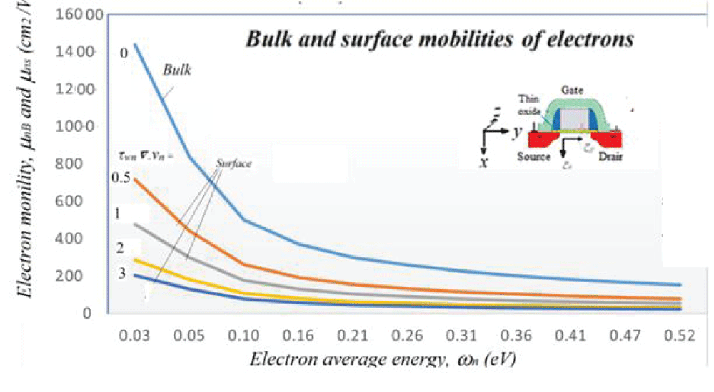
According to (12a), the mobility reduction due to the bulk hot electrons, increases when adding velocity gradient terms. For instance, consider the 2D planar MOSFET in the insert of the following figure. Here, we can consider only one velocity gradient component, namely, the off-diagonal elements (vnxvny∂vny/∂ x). For the matter of illustration, consider the following approximation:
(12b)
where the factor yn = an(ωn/ωo -1) with
, denoting the reduction due to bulk hot carriers (yn =µno/
). This factor is tightly related to the heating effect of the parallel field ζ// (and hence the drain-to-source bias voltages. Also, the factor
denotes the additional reduction in drift mobility, due to surface effects carriers (xn =no/ino). It can be written as follows near the surface of a 2D planar MOSFET
with
where we made two successive substitutions; the first is to assume the same energy dependence of the electron average mass and energy-relaxation time:
, and the second is to let µno = e τmno/mno. Note that the subscript i denotes the low-energy value near the bottom of conduction band. Also, the normalized velocity (
) may be assumed as slowly varying with electron energy Therefore, we can consider the pre-factor ßn independent of electron energy. Figure 2 depicts the variation of bulk and surface mobilities of electrons as a function of average electron energy for various values of the parameter (τwn ∂vny/∂ x). This normalized parameter characterizes the electron gas viscosity and hence the semiconductor surface roughness.
Figure 2: Plot of the surface degradation effects on the hot carrier mobility, near the Si/ SiO2 interface of an n-channel MOSFET, at various values of the velocity gradient. Here, we tak ðn around its median value ½ the upper curve shows the bulk mobility, with no velocity gradient.
iii. Comparison with Field-dependent Surface Mobility Models
For the matter of comparison of our mobility model with conventional field-dependent surface mobility models, let’s consider our surface mobility model (due to velocity gradients and surface roughness effects). As
, we can write
(13a)
Now, to compare this hydrodynamic model with the previous field-dependent surface mobility models, we need to some sort of a functional relational between the velocity gradient, ∂vny/∂ x to the normal field, ζ┴, across the channel of a MOSFET...
The easiest method to coincide between (13a) and the off-diagonal channel mobility component due to the normal field, ζ┴, µnvx = vny/ζ┴. As vny = Jn y/n, we can wrte
(13b)
Where,
is a critical normal field value. Near the top surface of the channel, we can assume
which is constant because ∇.Jn = 0. However, ζc is still position-dependent, because n = n(x). A more elaborate relation can be found by expanding n(x) as a function of ζ┴ , that’s n = f(ζ┴). Keeping the first order expansion term (
), results in:
(13c)
Where,
and ts is the average thickness of the channel inversion layer. The expansion n = f(ζ┴) at a certain lateral point y = yo, along the channel, can be calculated numerically from the tables of n(x) and ζ┴(x), which can be obtained by any semiclassic or quantum (S-P) solver [32]. Comparing (13c) with (13a), we get the thought functional relation:
(14)
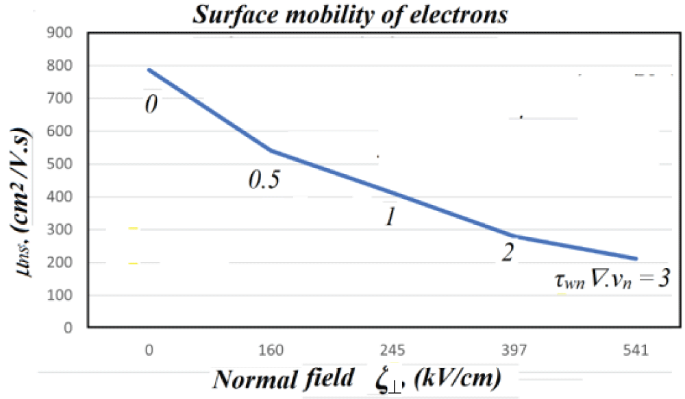
To plot µns(ζ┴ ), we proceed as follows: we extract the x-position dependent surface mobility, at different values of the parameter (xn = 2 τwn∇.vn), from Figure 3, at fixed values of ωn. This is done by drawing vertical lines at different values of ωn, which represent different points along the channel. Therefore, for each line we get the surface mobility µns at a specific value of nn. We then transform the nn value to an equivalent field value using our pilot model. The transformation can be done by the aid of our definition of ζc or, alternatively, by a fixed value, like that used in Yamaguchi model (4a), where ζc is fixed (ζc = 14.9kV/cm for electrons in Si at 300K). In fact, this value represents a specific device structure with specific bias conditions. The extracted plots of the x-position dependent µns(ζ┴) for a fixed values of ωn (one of them is shown in Figure 3), can be then averaged to obtain the effective surface mobility versus effective normal field.
Figure 2: Electron surface mobility versus normal field, across the channel at a lateral point of the channel where the average electron energy (ωn =20ωo). The low-field mobility of electrons is taken as 1450 cm2/V.s.
The final relation of effective mobility versus effective normal field is plotted together with some published values, in Figure 4. The figure shows our mobility model at the Si/SiO2 interface of an n-channel MOSFET and other published data of the so-called universal surface mobility [41], versus the effective normal fields. As shown, our model coincides with the measured mobility at a wide range of normal fields. In fact, the surface mobility is indeed limited by the electron gas viscosity due to surface friction (or the so-called roughness scattering) at high fields. The discrepancy from the measured data may be attributed to the fact that we considered only-energy-dependent energy relaxation time [40-43]. Actually, the energy relaxation time should lump the effect of the scattering mechanisms, which are position and temperature dependent, and may be more or less important near the semiconductor surface.
Figure 4: Comparison between the new mobility model at the Si/ SiO2 interface of an n-MOSFET and some published data at different substrate doping, versus effective surface field [23,41]. All data sets at Vsub=0, except the last one at Vsub= -3V.
V. Role of the Carrier Temperature Gradients
In order to simulate correctly the dynamic behaviors of hot carrier transport across a semiconductor interface region, we need to consider dynamic change of carrier density, velocity and energy (or temperature). The electron temperature gradient term in (8) is significant for hot and cold carriers transport around semiconductor junctions and interfaces. For instance, when electrons are accelerated and heated up after crossing into a high field region (e.g., across a potential barrier), their drift mobility will decrease. On the other hand, the hot electron drift mobility will increase after leaving a high field region and cooled down, unless it is decreased by other scattering mechanisms (e.g. higher impurity concentrations).
The carrier average mass gradients
The semiconductor band structure influences the carrier transport properties in semiconductor devices, and its effect are readily incorporated into our model through the energy-dependent physical parameters, such as the energy relaxation time, τwn(ꞷn), and the average carrier mass, mn(ꞷn), as well as its divergence. The consideration of the band structure in our mobility model is quite clear from the definition of the inverse mass tensor (1d).
Obviously, the average mass of electrons changes near semiconductor surfaces (due to the rupture of the periodicity of the crystal structure and the underlying surface states). Changes. Also, the average mass around the semiconductor heterojunctions, as well as 2DEG devices. Therefore, the average mass and its gradient are expected to influence the drift mobility in many semiconductor devices [44].
On the other hand, the effect of strain on the electron mobility can be understood in terms of the modification of the semiconductor band structure [45] and can be also included through the average mass and its gradient terms. In addition, the effect of crystal orientation on the drift mobility is tightly related to the average mass tensor, whose components change with the crystal direction. However, in the bulk of an isotropic semiconductor, the gradient term
in our mobility model is slowly varying with distance and can be neglected.
vii. Role of the carrier density gradients
The carrier density gradients are indeed important near the semiconductor surface and around the semiconductor interface regions (e.g., around a p-n junction). However, the density gradient coefficient (
) implies a mobility variation of
, which is much slower than the variation of ∇n.
viii. Role of the Carrier Heat Flux
The carrier heat flux can be expressed in terms of the carrier density and temperature gradients. This is clear in the simple Fourier relation (
) and our advanced model [46]. However, the divergence of the carrier heat flux has higher order gradients, which may be negligible with respect to other first gradient terms.
Conclusion
In this paper, we presented a surface mobility model for charge carriers in semiconductor devices and sensors, which is fully hydrodynamic and truly non-local. The model focuses on the reduction of drift mobility near semiconductor surfaces and around interface regions. Such a physics-based model will promote the role of high-order transport models (like the semiclassical and quantum hydrodynamic models). In fact, all previous surface mobility models where electric field dependent. Physically speaking, the hot carrier mobility should not be related to the local field, but rather to the carrier energy. In particular, the proposed model enables the HDM to handle the harsh problem of surface roughness scattering mechanism, through the viscosity of the hot electron gas near the surface. In fact, there are substantial number of analytical and numerical field-dependent models which describe the drift mobility near the surface of a semiconductor (Table 1). The local models were originally introduced to describe the mobility of carriers in the inversion layer of MOSFET devices, as a function of the applied electric field [9-18]. Unfortunately, these models cannot handle the non-local effects in nano-scale devices. In addition, the previous surface mobility models were primarily based on fitting the experimental data, which may change with the device technology node. Our non-local model of the hot carrier drift mobility is suitable for elemental and compound semiconductor devices and can be incorporated into both semiclassical and quantum hydrodynamic device simulators. In particular, the proposed model considers the velocity gradient of charge carriers, which is extremely important to simulate the nonlinear transport across barriers and Si/SiO2 interfaces, two of the most tedious problems in semiconductor device simulation. The model can be also helpful in the development of very high-speed 2-D transistors [47]. For the matter of comparison, we developed a pilot model relating the carrier velocity diversion to the normal fields in the channel of a MOSFET device, and found a good agreement, with some experimental results. Of course, more investigations and comparisons with experimental data and other models should be carried out.
Table 1: Comparison of hot-carrier mobility models.
Mobility model
Equations
Ref.
Notes
Yamaguchi
model
[20]
Field dependent, Bulk & surface
Darwish
model
[24]
Field dependent, Bulk & surface
Hansch-Mattausch model
[37]
Energy dependent, Bulk only
Our model
(reduced)
Energy and velocity gradient dependent, Bulk & surface
Our model
(generalized)
Energy & all gradients dependent, Bulk & surface & junctions.
El-Saba MH. Transport of Information-Carriers in Semiconductors and Nanodevices. PA, USA: IGI Global Publisher; 2017. Available from: https://www.igi-global.com/book/transport-information-carriers-semiconductors-nanodevices/173677
Hess K, Leburton JP, Ravaioli U, editors. Hot Carriers in Semiconductors. Springer; 1996.
Fischetti MV, Vandenberghe WG. Overview of Quantum-Transport Formalisms. In: Advanced Physics of Electron Transport in Semiconductors and Nanostructures. Graduate Texts in Physics. 361-380; 2016.
Martinez, Bescond M, Barker JR, Svizhenko A, Anantram MP, Millar C, Asenov A. A self-consistent full 3-D real-space NEGF simulator for studying nonperturbative effects in nano-MOSFETs. IEEE Trans Electron Devices. 2007;54(9):2213–2222.
Cerciganani A. The Boltzmann Equation and its Applications. Vienna: Springer-Verlag; 1988.
Rupp K. Deterministic Numerical Solution of the Boltzmann Transport Equation [Ph.D. Dissertation]. TUV, Wien; 2011. Available from: http://www.iue.tuwien.ac.at/phd/rupp/
Jacoboni C, Lugli P. The Monte Carlo Method for Semi-conductor Device Simulation. Springer Science and Business Media; 2012.
Vasileska D, Raleva K, Goodnick SM, Ringhofer C, Ahmed SS, Ashraf N, Hossain A, Hathwar R, Ashok A, Padmanabhan B. Monte Carlo Device Simulations. In: Applications of Monte Carlo Method in Science and Engineering. InTech; 2011. DOI: 10.5772/16190
Vasicek M. Advanced Macroscopic Transport Models [Dissertation]. Technische Universität Wien; 2009.
El-Saba MH, Taha MS. An Ultimate Hydrodynamic Model for Semiconductor Devices, Including Band Structure and Surface Effects. Sensors and Actuators Magazine. 2024;267(4).
Sabbah AJ, Riffe DM. Femtosecond Pump-Probe Reflectivity Study of Silicon Carrier Dynamics. Phys Rev B. 2002;66:165217-165228.
Takagi S, Toriumi A, Iwase M, Tango H. On the Universality of Inversion Layer Mobility in Si MOSFET’s: Part I – Effects of Substrate Impurity Concentration. IEEE Transactions on Electron Devices. 1994;41(12):2357-2362.
EL-SABA MH. Hydrodynamic Modeling and Simulation of Hot Carrier Transport Phenomena and Impact Ionization in Semiconductor Devices [Ph.D. Dissertation]. INSA Lyon, France; 1993. Order No.93 ISAL 0072.
Takagi S, Toriumi A, Iwase M, Tango H. On the universality of inversion layer mobility in Si MOSFET’s: part II—effects of surface orientation. IEEE Trans Electron Dev. 1994;41(12):2363–2368.
Gardner C. The quantum hydrodynamic model for semiconductor devices. SIAM Journal on Applied Mathematics. 1994;54(2):409–427.
Spinelli AS. Self-consistent 2-D model for quantum effects in n-MOS transistors. IEEE Trans Electron Devices. 1998.
Ferry DK, Ramey S, Shifren L, Alkis E. The Effective Potential in Device Modeling: The Good, the Bad and the Ugly. Journal of Comp Electron. 2002;1(1):9–65.
Asenov A, Brown AR, Watling JR. Quantum Corrections in the Simulation of Decanano MOSFETs. Solid-State Electron. 2003;47(7):1141-1145.
Yue C, Agostinelli V, Yeric GM, Tasch A. Improved universal MOSFET electron mobility degradation models for circuit simulation. IEEE Transactions on Computer Aided Design. 1993;12(10).
Yamaguchi K. Field-Dependent Mobility Model for Two-Dimensional Numerical Analysis of MOSFET's. IEEE Trans Electron Devices. 1979;26:1068-1074.
Caughey DM, Thomas RE. Carrier Mobilities in Silicon Empirically Related to Doping and Field. Proc IEEE. 1967:2192–93.
Nishida T, Sah CT. A physically based mobility model for MOSFET numerical simulation. IEEE Transactions on Electron Devices. 1987;34(2).
Donetti L, Gamiz F, Rodriguez N, Godoy A. Hole mobility in ultrathin double-gate SOI devices: the effect of acoustic phonon confinement. IEEE electron device letters. 2009;30(12):1338-1340.
Darwish MN, Lentz JL, Pinto MR, Zeitzoff PM, Krutsick TJ, Vuong HH. An Improved Electron and Hole Mobility Model for General Purpose Device Simulation. IEEE Trans Electron Dev. 1997;44(9):1529-1538.
Klassen DB. A unified mobility model for device simulation-Part I: Model equations and concentration dependence. Solid-State Electron. 1992;35(7):953-959.
Lombardi C, Manzini S, Saporito A, Vanzi M. A physically based mobility model for numerical simulation of nonplanar devices. IEEE Trans Computer-Aided Design. 1988;7:1164–1171.
Gamiz F, Lopez-Villanueva JA, Banqueri J, Carceller J, Cartujo P. Universality of electron mobility curves in MOSFET’s: A Monte Carlo study. IEEE Trans Electron Devices. 1995;42:258.
Esseni D. On the Modeling of Surface Roughness Limited Mobility in SOI MOSFETs and its Correlation to the Transistor Effective Field. IEEE Trans Electron Devices. 2004;51:394-401.
Weber O, Takagi S. New Findings on Coulomb Scattering Mobility in Strained-Si nFETs and its Physical Understanding. Symposium on VLSI Technology Digest. 2007:130-131.
Gamiz F, López-Villanueva JA, Roldan JB. Monte Carlo simulation of electron transport properties in extremely thin SOI MOSFET's. IEEE Transactions on Electron Devices. 2009;45(5):1122–1126.
Naydenov K, Donato N, Udrea F. An advanced physical model for the Coulombic scattering mobility in 4H-SiC inversion layers. Journal of Applied Physics. 2020;127:194504.
Balaguer M, Roldan JB, Donetti L, Gamiz F. Inversion charge modeling in n-type and p-type Double-Gate MOSFETs including quantum effects: The role of crystallographic orientation. Solid-state electronics. 2012;67(1):30-37.
Reggiani S, Valdinoci M, Colalongo L, Baccarani G. A Unified Analytical Model for Bulk and Surface Mobility in Si n-and p-Channel MOSFET's. Proc European Solid-State Device Research Conf. 1999;1.
El-Saba MH. Accurate Estimation of Electron Velocity Overshoots in Sub-0.1 micron Silicon Structures and MOSFET Devices. Proceedings of the 15th Radio Science Conference, NRSC '98. 1998:D2/1 - D2/5.
El-Saba MH. Investigation of Hot Carrier Repelling Effect in Semiconductor Devices, Using an Analytical Solution of the Hydrodynamic Model. IEEE Trans Electron Devices. 2006;53(7):1615-1622.
El-Saba MH. Yet another Hydrodynamic Model for Silicon Devices with Correlated Parameters. Scientific & Academic Publishers, Microelectronic Devices and Solid-State Electronics. 2012;1(5):118-147.
Hansch W, Miura-Mattausch M. The Hot-Electron Problem in Small Semiconductor Devices. Journal of Applied Physics. 1986;60(2):650-656.
Gonzalez B, Palankovski V, Kosina H, Hernandez A, Selberherr S. An energy relaxation time model for device simulation. Solid-state electronics. 1999;43(9):1791-1795.
Vasileska D, Goodnick S, Klimeck G. Computational Electronics: Semi-Classical and Quantum Device Modeling and Simulation. CRC Press; 2010.
El-Saba MH, Taha MS. Hydrodynamic Modeling of the 2DEG/2DHG viscosity, as a function of the electron/hole temperature. To be published. 2023.
Watt JT, Plummer JD. Universal Mobility-Field Curves for Electrons and Holes in MOS Inversion Layers. 1987 Symposium on VLSI Technology. Digest of Technical Papers, Karuizawa, Japan. 1987:81-82.
Sasso G, Rinaldi N, Matz G, Jungemann C. Accurate Mobility and Energy Relaxation Time Models for SiGe HBTs Numerical Simulation. 2009 International Conference on Simulation of Semiconductor Processes and Devices, San Diego, CA, USA. 2009:1-4.
Dolgopolov VT, Shashkin AA, Dorozhkin SI, Vyrodov EA. Energy relaxation time in a two-dimensional electron gas at a (001) surface of silicon. JETP, Theor. Fi. 1985;89:2113-2123.
Sho S, Odanaka S. A quantum energy transport model for semiconductor device simulation. Journal of Computational Physics. 2013;235:486–496.
Wang X, Xu X, Wang H. Analytical model for uniaxial strained Si inversion layer electron effective mobility. IET Circuits, Devices & Systems. 2019;13(3):414-419.
El-Saba MH. Problems Related to the Semiconductors Hydrodynamic Model: Modeling the Carrier-Heat Flux Term. Proc of the 8th Int Conf on Microelectronics-ICM, M. El-Masry (Ed.), Cairo. 1996:162–166.
Mir SH, Yadav VK, Singh JK. Recent Advances in the Carrier Mobility of Two-Dimensional Materials: A Theoretical Perspective. ACS Omega. 2020;5(24):14203-14211.
El-Saba MH, Taha MS. A Unified Mobility Model for Semiconductor Devices and Sensors, Including Surface Hydrodynamic Viscosity. IgMin Res. June 25, 2025; 3(6): 239-250. IgMin ID: igmin305; DOI:10.61927/igmin305; Available at: igmin.link/p305
Ain-Shams University Engineering College, 15117 Abbasya, Cairo, Egypt
Address Correspondence: Muhammad H El-Saba, Ain-Shams University Engineering College, 15117 Abbasya, Cairo, Egypt, Email: [email protected]
How to cite this article: El-Saba MH, Taha MS. A Unified Mobility Model for Semiconductor Devices and Sensors, Including Surface Hydrodynamic Viscosity. IgMin Res. June 25, 2025; 3(6): 239-250. IgMin ID: igmin305; DOI:10.61927/igmin305; Available at: igmin.link/p305
Figure 1: Electron drift mobility in the homogenous bulk of ...
Figure 2: Plot of the surface degradation effects on the hot...
Figure 3: Electron surface mobility versus normal field, acr...
Figure 4: Comparison between the new mobility model at the S...
El-Saba MH. Transport of Information-Carriers in Semiconductors and Nanodevices. PA, USA: IGI Global Publisher; 2017. Available from: https://www.igi-global.com/book/transport-information-carriers-semiconductors-nanodevices/173677
Hess K, Leburton JP, Ravaioli U, editors. Hot Carriers in Semiconductors. Springer; 1996.
Fischetti MV, Vandenberghe WG. Overview of Quantum-Transport Formalisms. In: Advanced Physics of Electron Transport in Semiconductors and Nanostructures. Graduate Texts in Physics. 361-380; 2016.
Martinez, Bescond M, Barker JR, Svizhenko A, Anantram MP, Millar C, Asenov A. A self-consistent full 3-D real-space NEGF simulator for studying nonperturbative effects in nano-MOSFETs. IEEE Trans Electron Devices. 2007;54(9):2213–2222.
Cerciganani A. The Boltzmann Equation and its Applications. Vienna: Springer-Verlag; 1988.
Rupp K. Deterministic Numerical Solution of the Boltzmann Transport Equation [Ph.D. Dissertation]. TUV, Wien; 2011. Available from: http://www.iue.tuwien.ac.at/phd/rupp/
Jacoboni C, Lugli P. The Monte Carlo Method for Semi-conductor Device Simulation. Springer Science and Business Media; 2012.
Vasileska D, Raleva K, Goodnick SM, Ringhofer C, Ahmed SS, Ashraf N, Hossain A, Hathwar R, Ashok A, Padmanabhan B. Monte Carlo Device Simulations. In: Applications of Monte Carlo Method in Science and Engineering. InTech; 2011. DOI: 10.5772/16190
Vasicek M. Advanced Macroscopic Transport Models [Dissertation]. Technische Universität Wien; 2009.
El-Saba MH, Taha MS. An Ultimate Hydrodynamic Model for Semiconductor Devices, Including Band Structure and Surface Effects. Sensors and Actuators Magazine. 2024;267(4).
Sabbah AJ, Riffe DM. Femtosecond Pump-Probe Reflectivity Study of Silicon Carrier Dynamics. Phys Rev B. 2002;66:165217-165228.
Takagi S, Toriumi A, Iwase M, Tango H. On the Universality of Inversion Layer Mobility in Si MOSFET’s: Part I – Effects of Substrate Impurity Concentration. IEEE Transactions on Electron Devices. 1994;41(12):2357-2362.
EL-SABA MH. Hydrodynamic Modeling and Simulation of Hot Carrier Transport Phenomena and Impact Ionization in Semiconductor Devices [Ph.D. Dissertation]. INSA Lyon, France; 1993. Order No.93 ISAL 0072.
Takagi S, Toriumi A, Iwase M, Tango H. On the universality of inversion layer mobility in Si MOSFET’s: part II—effects of surface orientation. IEEE Trans Electron Dev. 1994;41(12):2363–2368.
Gardner C. The quantum hydrodynamic model for semiconductor devices. SIAM Journal on Applied Mathematics. 1994;54(2):409–427.
Spinelli AS. Self-consistent 2-D model for quantum effects in n-MOS transistors. IEEE Trans Electron Devices. 1998.
Ferry DK, Ramey S, Shifren L, Alkis E. The Effective Potential in Device Modeling: The Good, the Bad and the Ugly. Journal of Comp Electron. 2002;1(1):9–65.
Asenov A, Brown AR, Watling JR. Quantum Corrections in the Simulation of Decanano MOSFETs. Solid-State Electron. 2003;47(7):1141-1145.
Yue C, Agostinelli V, Yeric GM, Tasch A. Improved universal MOSFET electron mobility degradation models for circuit simulation. IEEE Transactions on Computer Aided Design. 1993;12(10).
Yamaguchi K. Field-Dependent Mobility Model for Two-Dimensional Numerical Analysis of MOSFET's. IEEE Trans Electron Devices. 1979;26:1068-1074.
Caughey DM, Thomas RE. Carrier Mobilities in Silicon Empirically Related to Doping and Field. Proc IEEE. 1967:2192–93.
Nishida T, Sah CT. A physically based mobility model for MOSFET numerical simulation. IEEE Transactions on Electron Devices. 1987;34(2).
Donetti L, Gamiz F, Rodriguez N, Godoy A. Hole mobility in ultrathin double-gate SOI devices: the effect of acoustic phonon confinement. IEEE electron device letters. 2009;30(12):1338-1340.
Darwish MN, Lentz JL, Pinto MR, Zeitzoff PM, Krutsick TJ, Vuong HH. An Improved Electron and Hole Mobility Model for General Purpose Device Simulation. IEEE Trans Electron Dev. 1997;44(9):1529-1538.
Klassen DB. A unified mobility model for device simulation-Part I: Model equations and concentration dependence. Solid-State Electron. 1992;35(7):953-959.
Lombardi C, Manzini S, Saporito A, Vanzi M. A physically based mobility model for numerical simulation of nonplanar devices. IEEE Trans Computer-Aided Design. 1988;7:1164–1171.
Gamiz F, Lopez-Villanueva JA, Banqueri J, Carceller J, Cartujo P. Universality of electron mobility curves in MOSFET’s: A Monte Carlo study. IEEE Trans Electron Devices. 1995;42:258.
Esseni D. On the Modeling of Surface Roughness Limited Mobility in SOI MOSFETs and its Correlation to the Transistor Effective Field. IEEE Trans Electron Devices. 2004;51:394-401.
Weber O, Takagi S. New Findings on Coulomb Scattering Mobility in Strained-Si nFETs and its Physical Understanding. Symposium on VLSI Technology Digest. 2007:130-131.
Gamiz F, López-Villanueva JA, Roldan JB. Monte Carlo simulation of electron transport properties in extremely thin SOI MOSFET's. IEEE Transactions on Electron Devices. 2009;45(5):1122–1126.
Naydenov K, Donato N, Udrea F. An advanced physical model for the Coulombic scattering mobility in 4H-SiC inversion layers. Journal of Applied Physics. 2020;127:194504.
Balaguer M, Roldan JB, Donetti L, Gamiz F. Inversion charge modeling in n-type and p-type Double-Gate MOSFETs including quantum effects: The role of crystallographic orientation. Solid-state electronics. 2012;67(1):30-37.
Reggiani S, Valdinoci M, Colalongo L, Baccarani G. A Unified Analytical Model for Bulk and Surface Mobility in Si n-and p-Channel MOSFET's. Proc European Solid-State Device Research Conf. 1999;1.
El-Saba MH. Accurate Estimation of Electron Velocity Overshoots in Sub-0.1 micron Silicon Structures and MOSFET Devices. Proceedings of the 15th Radio Science Conference, NRSC '98. 1998:D2/1 - D2/5.
El-Saba MH. Investigation of Hot Carrier Repelling Effect in Semiconductor Devices, Using an Analytical Solution of the Hydrodynamic Model. IEEE Trans Electron Devices. 2006;53(7):1615-1622.
El-Saba MH. Yet another Hydrodynamic Model for Silicon Devices with Correlated Parameters. Scientific & Academic Publishers, Microelectronic Devices and Solid-State Electronics. 2012;1(5):118-147.
Hansch W, Miura-Mattausch M. The Hot-Electron Problem in Small Semiconductor Devices. Journal of Applied Physics. 1986;60(2):650-656.
Gonzalez B, Palankovski V, Kosina H, Hernandez A, Selberherr S. An energy relaxation time model for device simulation. Solid-state electronics. 1999;43(9):1791-1795.
Vasileska D, Goodnick S, Klimeck G. Computational Electronics: Semi-Classical and Quantum Device Modeling and Simulation. CRC Press; 2010.
El-Saba MH, Taha MS. Hydrodynamic Modeling of the 2DEG/2DHG viscosity, as a function of the electron/hole temperature. To be published. 2023.
Watt JT, Plummer JD. Universal Mobility-Field Curves for Electrons and Holes in MOS Inversion Layers. 1987 Symposium on VLSI Technology. Digest of Technical Papers, Karuizawa, Japan. 1987:81-82.
Sasso G, Rinaldi N, Matz G, Jungemann C. Accurate Mobility and Energy Relaxation Time Models for SiGe HBTs Numerical Simulation. 2009 International Conference on Simulation of Semiconductor Processes and Devices, San Diego, CA, USA. 2009:1-4.
Dolgopolov VT, Shashkin AA, Dorozhkin SI, Vyrodov EA. Energy relaxation time in a two-dimensional electron gas at a (001) surface of silicon. JETP, Theor. Fi. 1985;89:2113-2123.
Sho S, Odanaka S. A quantum energy transport model for semiconductor device simulation. Journal of Computational Physics. 2013;235:486–496.
Wang X, Xu X, Wang H. Analytical model for uniaxial strained Si inversion layer electron effective mobility. IET Circuits, Devices & Systems. 2019;13(3):414-419.
El-Saba MH. Problems Related to the Semiconductors Hydrodynamic Model: Modeling the Carrier-Heat Flux Term. Proc of the 8th Int Conf on Microelectronics-ICM, M. El-Masry (Ed.), Cairo. 1996:162–166.
Mir SH, Yadav VK, Singh JK. Recent Advances in the Carrier Mobility of Two-Dimensional Materials: A Theoretical Perspective. ACS Omega. 2020;5(24):14203-14211.






 Scan and get link
![Electron drift mobility in the homogenous bulk of undoped silicon at 300K, versus electron average energy, according to our model. The energy relaxation time of electrons in Si, is plotted on the secondary axis, as a function of electron energy according to [39].](https://www.igminresearch.com/articles/figures/igmin305/igmin305.g001.png)
![Comparison between the new mobility model at the <em>Si/ SiO<sub>2</sub></em> interface of an n-MOSFET and some published data at different substrate doping, versus effective surface field [23,41]. All data sets at <em>V<sub>sub</sub></em>=0, except the last one at <em>V<sub>sub</sub></em>= -3V.](https://www.igminresearch.com/articles/figures/igmin305/igmin305.g004.png)